|
In Architecture as in all other Operative Arts, the end must direct the Operation. The end is to build well.
The CVD growth of silicon (001) from disilane (Si2H6) has been studied using a variety of surface science techniques (Gates 1988; Gates, Greenlief and Beach 1990; Gates 1992; Liu et al. 1992; Mokler et al. 1992; Kolasinski et al. 1992), which have given an understanding of the process on a macroscopic scale, including the rate and results of growth. Disilane is a promising candidate for low temperature CVD growth because it has a relatively high sticking coefficient, and a low activation energy for breaking the Si-Si bond. This means that it can be used for growth without the presence of an activator such as chlorine, as is necessary in the case of, for instance, SiH4 (Gates 1988).
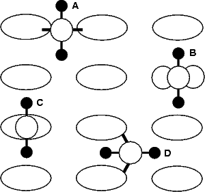
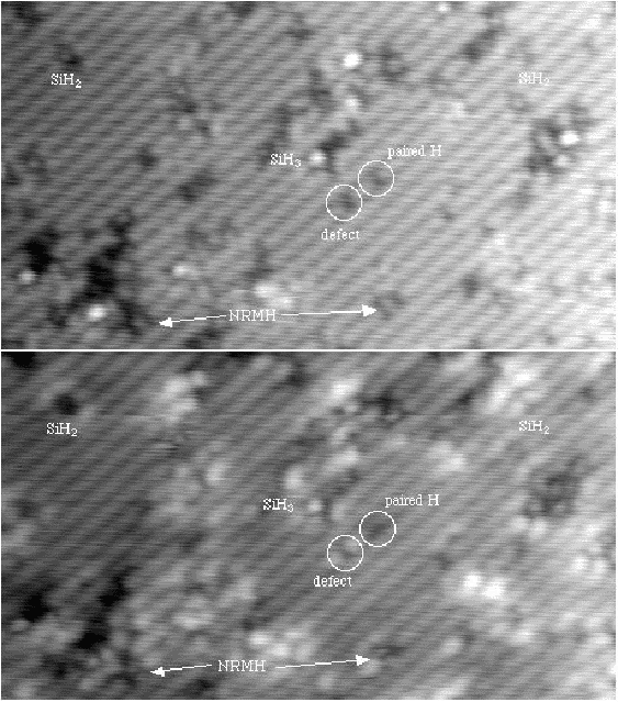
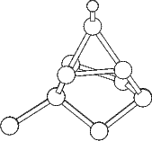
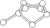
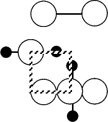
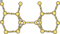
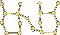
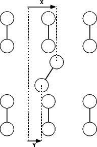
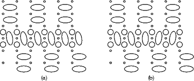
Scanning tunneling microscopy (STM) studies (Boland 1991; Lin et al. 1992; Bronikowski et al. 1993; Wang, Bronikowski and Hamers 1994; Owen et al. 1997a,b) have begun to give a real-space understanding of the detailed chemistry of disilane on silicon, and the initial stages of adsorption, dissociation and epitaxial growth. Boland (1991) studied the role of hydrogen on the silicon surface in the adsorption and dissociation of disilane, and showed that growth at high hydrogen coverage is governed by the reactions of disilane with the hydrogenated surface. He also observed that the result of annealing a disilane-saturated surface was strips of epitaxial dimer rows. Lin et al. (1992) studied adsorption at 350oC, and observed the formation of anisotropic islands, which they attributed to silicon dimers saturated with hydrogen. While they found that the fragments from disilane adsorption were randomly distributed, they did not identify the nature of these fragments. Bronikowski et al. (1993) identified the initial product as adsorbed SiH3, which quickly breaks down to form SiH2, with a hydrogen left on the surface. After postulating four candidate sites for the SiH2 adsorption (shown in Fig. 7.2), they identified the actual bonding site from the geometry of the adsorbed fragment. A typical image of the Si(001) surface after adsorption of a small quantity of disilane is shown in Figure 7.1. SiH2 refers to a fragment resulting from disilane adsorption bonded in the intra-row configuration (C in Figure 7.2), SiH3 is the precursor to this, NRMH is a non-rotated (i.e. non-epitaxial) monohydride dimer, and defects and paired hydrogens have been discussed in previous chapters. The images are at different biases, which enables the defects (which show an enhancement) to be differentiated from the paired hydrogen (which don’t).
|
In a later study, Wang, Bronikowski and Hamers (1994) investigated the initial stages of epitaxial growth which proceed from this adsorbed fragment. They suggested a mechanism whereby two SiH2 groups in position D in Figure 7.2 on adjacent rows bond to form a hydrogenated dimer, and lose an H2 molecule. The only hydrogenated dimers which they observed were non-rotated, that is, parallel to the dimers in the surface.
In this section, the total energies calculated using LDA for an SiH2 fragment in the four possible bonding sites in Fig.7.2 are presented, two of which prove to be very close in energy (Bowler and Goringe 1996). The energy for a second adsorbate, and therefore the interaction energies implied by this, have also been evaluated. The results imply that epitaxial hydrogenated dimers cannot form directly from SiH2, but that the mechanism proposed by Wang, Bronikowski and Hamers (1994) for the formation of non-rotated hydrogenated dimers is plausible; it will be considered in Section 7.3.
A standard unit cell was used, with one SiH2 fragment on the top surface. A vacuum slab of at least 7 Å was used to ensure decoupling of periodic images. A disilane molecule was relaxed in isolation for purposes of comparison.
The energies for the four different structures, and details of bond lengths and angles are given in Table 7.1. As can be seen, both the intra-row structure and the on-dimer structure are plausible candidates for the lowest energy structure.
| |||||||||||||||||||||||||||||||||||||||||||||||||||||||||||||||
 -bond is
broken.
-bond is
broken.
There are two structures which have energies that make them plausible candidates for the stable adsorption site:
the on-dimer and the intra-row. The on-dimer structure was discarded by Bronikowski et al. (1993), on the grounds
that the angles in the structure (63o in Table 7.1) were sterically unfavourable. However, as shown in Table 7.1, the
energy is nearly comparable with the intra-row structure. A possible reason for this stability is that the intra-row
structure breaks the  -bonds on two dimers, and saturates only one dangling bond on each, whereas the on-dimer
structure breaks the -bond on only one dimer, and saturates both dangling bonds on that dimer. Bond angles close
to sixty degrees are seen elsewhere in silicon chemistry : in the angular distribution for liquid silicon, a clear peak
can be seen at 60 degrees (Horsfield and Clancy 1994); the bond angle formed between the silicon dimer and the
Si-C bond when C2H2 and C2H4 adsorb on silicon is 73 and 75 degrees respectively (Andrew Fisher,
Private Communication); and with a silicon interstitial defect, many of the angles formed are about 60
degrees.
-bonds on two dimers, and saturates only one dangling bond on each, whereas the on-dimer
structure breaks the -bond on only one dimer, and saturates both dangling bonds on that dimer. Bond angles close
to sixty degrees are seen elsewhere in silicon chemistry : in the angular distribution for liquid silicon, a clear peak
can be seen at 60 degrees (Horsfield and Clancy 1994); the bond angle formed between the silicon dimer and the
Si-C bond when C2H2 and C2H4 adsorb on silicon is 73 and 75 degrees respectively (Andrew Fisher,
Private Communication); and with a silicon interstitial defect, many of the angles formed are about 60
degrees.
The silicon-hydrogen bonds are, in all cases, within 1% of the length in the isolated Si2H6 molecule (1.53Å),
which suggests that there has been very little change in the nature of the bonding. The adsorbate-dimer bond
lengths in Table 7.1 can also be compared with Si2H6, in which the silicon-silicon bond length is found to be 2.31 Å.
In the intra-row structure, this bond has been lengthened by about 4%; this is due to the geometric strain, and is a
further reason for the relative stability of the on-dimer structure. The dimer bonds are slightly lengthened when
compared to the clean dimer length (2.37 Å) as a result of the partial breaking of the -bond referred to
above.
|
|
|
|
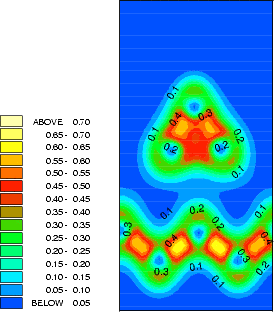
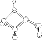
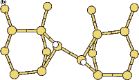
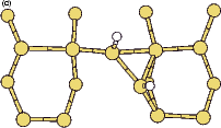
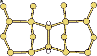
The structure and charge densities for the two minimum energy sites, with a clean dimer displayed for
comparison, are shown in Fig.7.3-7.5. For the on-dimer structure (Fig.7.3), the bonds between the adsorbed silicon
and the dimer atoms are as strong as a dimer bond despite the unfavourable angles, while the bond between
the dimer atoms is weakened and lengthened (c.f. Table 7.1). The intra-row structure (Fig.7.4) has a
four-membered ring. The bonds between the adsorbed silicon and the dimer atoms are as strong as the
back-bonds, and indeed resemble them rather closely. In each case, the dimer bond length is increased
somewhat compared to the clean dimer (2.37 Å). This is characteristic of the removal of the dimer
-bond.
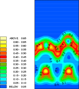
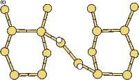
Bronikowski et al. (1993) noted that the SiH2 fragment did not cause the dimers in its immediate vicinity to be pinned. Their explanation for this involved the electronic states of the dimers on which the fragment was adsorbed. Inspection of Fig.7.4 (the intra-row structure) suggests an alternative explanation: as the ends of the dimers on which the fragment is adsorbed (at the front) are at essentially the same height, and the other ends of the dimers (at the back) differ in height, there is no reason for the bare ends not to flip as clean dimers do. Indeed, in Figure 7.6 a contour plot of the charge density at the clean end of the dimers with the SiH2 fragment adsorbed is shown with the same plot for the clean surface shown for comparison. The charge densities are almost identical, suggesting that there is a degree of delocalisation around the dimer-SiH2-dimer system, causing the dimers to be linked and flip in concert. This will mean that the clean dimers in the vicinity are not pinned.
The next step in the growth of silicon from disilane is for two fragments to form a single dimer of monohydride, losing H2 in the process (Wang, Bronikowski and Hamers 1994). For this to take place, two SiH2 groups must first be adsorbed on adjacent sites. An interaction energy of two such groups can be defined as the energy of two groups adsorbed on adjacent sites minus the energy of two groups adsorbed independently. For the on-dimer structure, this interaction energy is +0.20 eV (a positive energy indicates a repulsive interaction) per adsorbed fragment. This is very similar to the case of C2H2 and C2H4 on silicon, where the molecules adsorb on alternate dimers (Fisher, Blöchl and Briggs 1997; Mayne et al. 1996), due to a positive interaction energy, though the source of the repulsion may well be completely different. This large positive interaction energy will prevent adsorption on adjacent sites for the on-dimer structure except at very high coverages. By contrast, the interaction energy for the intra-row structure is very close to zero (magnitude less than 0.01 eV) so there will be no such effect.
Geometrically, an epitaxial hydrogenated dimer could form from the two adjacent SiH2 fragments in the inter-row, in-dimer or on-dimer structures (see Fig.7.2). The first two of these structures are not energetically favourable even in isolation, and the repulsive interaction energy for the on-dimer structure prevents the adsorption of two SiH2 groups on adjacent dimers. Therefore, epitaxial hydrogenated dimers cannot form from SiH2 fragments.
A non-epitaxial hydrogenated dimer could form from two SiH2 fragments in the intra-dimer structure adsorbed on adjacent dimer rows. The mechanism which has been proposed by Wang, Bronikowski and Hamers (1994) involves the formation of a Si-Si bond and the elimination of H2, and is discussed in Section 7.3.
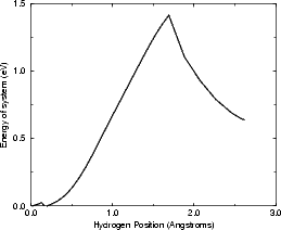
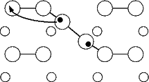
In solid source MBE of silicon, the species arriving at the surface is silicon adatoms. These are free to diffuse about the surface after deposition (with a low barrier of 0.7 eV (Swartzentruber 1996)), and quickly form long, thin islands of epitaxial silicon dimers. The same is not true for gas source MBE, where the species left adsorbed after deposition are SiH2 and H. The SiH2 groups are adsorbed randomly on the surface after adsorption (Wang, Bronikowski and Hamers 1994; Owen et al. 1997a), with no correlation in position. By 450 K, these fragments have rearranged to lie next to each other on adjacent dimer rows: clearly, they must have started to diffuse. There are at least three possible diffusion processes which could go on: on-dimer to on-dimer (along the top of the dimer rows); intra-row to intra-row (along the side of the dimer rows); and on-dimer to intra-row or vice versa (diagonally across the dimer rows). As there is such freedom of movement, the energy surface for the SiH2 group to diffuse along the dimer row with any of these process was evaluated using LDA, and is shown in Figure 7.7(a). The area of the surface considered is indicated in Fig. 7.7(b) with a dashed rectangle. A unit cell which was half of the standard unit cell (i.e. one dimer row wide) was used, with a single SiH2 fragment on the surface.
|
The surface shows classic saddle-point behaviour, with a minimum barrier of 1.1 eV to go from on-dimer to intra-row or vice versa (which is nicely in line with the temperature found experimentally at which these groups start to move). There is another possibility for diffusion from on-dimer to on-dimer, with a barrier of 1.4 eV (with Fig. 7.7(a) showing only the first half of the process) but this will be less likely. This suggests that, once sufficient thermal energy is available, the groups will diffuse up and down the rows. Two on-dimer groups on adjacent dimers will repel each other, and it is unlikely that two intra-row groups could reside on the opposite sides of the same pair of dimers; while energetically favourable, it would be sterically hindered. The monohydride formation discussed in the next section, where the reaction proceeds between two intra-row groups on adjacent dimer rows, will be the most likely formation reaction.
Once the SiH2 groups have been observed to rearrange on the surface, the next feature observed in STM is a non-rotated (i.e. non-epitaxial) monohydride group, across the trench between dimer rows. It is highly likely that these form from two SiH2 groups, which sit on adjacent dimer rows in the intra-row position. The reason that other orientations are not seen has been explained above - the on-dimer position has a repulsive interaction for two neighbouring groups, and the monohydride dimer on top of a dimer row is probably sterically hindered - the second group could not diffuse to sit in the appropriate position. As a point of comparison with clean dimers, the stabilities of monohydride dimers in the four positions available (on the dimer row and over the trench in both epitaxial and non-epitaxial positions) were modelled. These are shown in Table 7.2, and provide another interesting example of how vital the experimental-theoretical interaction can be: total energy calculations suggest that the most stable monohydride dimer, and thus the first candidate for modelling, is the epitaxial row dimer; only from experiment is it clear that the formation of the non-epitaxial trench dimer, third most stable structure, should be modelled.
|
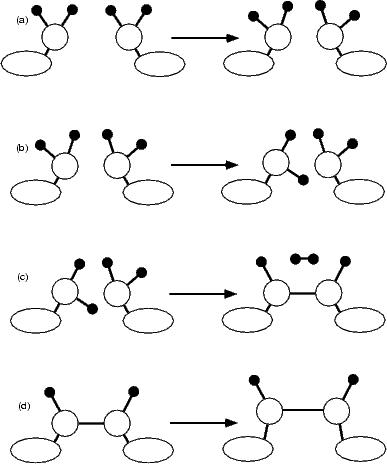
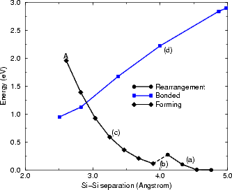
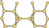
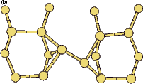
The reaction proceeds in three stages (shown schematically in Figure 7.8), for which the driving force is the steric repulsion of adjacent hydrogens. As the groups are pulled together initially, the SiH2 groups undergo little change, except for a slight rotation to bring the hydrogens upright (Fig. 7.8(a)). Once the separation reaches 3.8 Å, one of the groups undergoes a drastic rearrangement, rotating so that one hydrogen points directly into the trench between dimer rows, while the other continues to move so that the hydrogens are upright (Fig. 7.8(b)). This conformation is held as the groups are pulled together, until a silicon-silicon bond is formed and two of the hydrogens (one from each group) react to give an H2 molecule which is lost to the vacuum (Fig. 7.8(c)) in the calculation, or, in the STM experiment, to the gas phase. This is indicated with the letter A in Fig. 7.9.
|
|
The energy for these processes, along with that for stretching the dimer (Fig. 7.8(d)), is plotted in Figure 7.9. The reaction starts at the right hand side of the graph (as the separation is being decreased) and proceeds to the left. As can be seen, it is an endothermic reaction; however it is also irreversible, as the H2 molecule is lost to the vacuum once it is formed. The three stages of the formation reaction are indicated with circles and a solid line (for part (a) in Fig. 7.8), a dashed line (for part (b)), diamonds and a solid line (for part (c)), while the stretching mode (part (d)) is indicated with squares and a blue line. The reaction proceeds with a maximum barrier of 1.9 eV; however, there may well be a lower energy path with a barrier closer to the cross-over between the two processes, in the region of 1.4 eV. From these graphs, and the experimental evidence, the true barrier is estimated as 1.4±0.2eV, though all that can be conclusively said at present is that the barrier is between 1.2 and 1.9 eV. The difficulty is that the rearrangement during the formation of the Si-Si bond (Fig. 7.8(c)) is an extremely slow process, requiring many hundreds of steps in LDA, which is costly in computational terms. This is hard to explore correctly; with more resources, and a parallel implementation of the nudged elastic band method mentioned in Chapter 2, the modelling of the barrier could be improved. Nevertheless, the process appears to be reasonable given the available evidence.
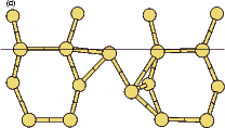
The rotation of a silicon dimer on top of the dimer rows has been observed and modelled in the past (Swartzentruber, Smith and Jónsson 1996); in this section, the DFT modelling of the rotation over the trench between dimer rows is discussed. This may have relevance to the process of conversion between the non-epitaxial monohydride dimers which are formed as discussed in the previous section and clean dimers which form the new layer of silicon, and this is touched on briefly at the end of the section. All of the calculations in this section used the standard unit cell, with a dimer (either clean or hydrogenated) placed over the trench between dimer rows.
|
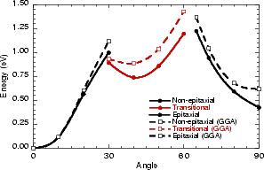
If this metastable, transitional structure is rotated further, it again spontaneously transforms into the epitaxial ad-dimer (which is metastable with respect to the non-epitaxial dimer) once the angle is taken past 65o (e). Thus the three domains of stability for the different structures are from 0o-30o, the non-epitaxial dimer; from 30o to 60o, the transitional structure; and from 60o to 90o, the epitaxial dimer. The energy barrier for the process is shown in Fig. 7.11, where the central lines denote the energy for the transitional structure, and the outer lines the energies for the non-epitaxial and epitaxial dimers.
|
The barrier to go from the non-epitaxial position to the transitional structure is 0.95 eV, and the barriers to go on from there are 0.2 eV to return to the non-epitaxial position, and 0.6 eV to go on into the epitaxial position. However, it seems more likely that the dimer will go straight from the non-epitaxial position to the epitaxial position (with a barrier of 1.2 eV) via the transitional structure, rather than residing in the transitional structure. The barrier in the opposite direction, i.e. to go from the epitaxial position to the transitional structure, is 0.95 eV and will not be changed by having to leave the transitional structure. The effect of gradient corrections is relatively small - only raising the overall barrier by 0.2 eV - though they do make the transitional structure less stable with respect to the non-epitaxial position.
|
|
The bonding at the top end of the dimer is quite peculiar. Figure 7.12 shows charge density contours taken in a plane containing the top pair of substrate dimers in Fig. 7.10, for three different angles. This plane is indicated with a thin line on the 60o (shifted) structure in Fig. 7.10(d). The process seen in the transition from the top to the bottom panel of Fig. 7.12 is the formation of a second bond between the rotating dimer and the substrate dimers; in the top panel, the ad-dimer atom (C) is at the same height as the substrate dimers (A, B and D, E), which would mean that it would form a pair of bonds with an angle between them of 180o. This would be highly unusual bonding for silicon, and indeed does not happen: despite the fact that the distances are almost identical, there is no bond between the ad-dimer and the right-hand substrate dimer. As the rotation proceeds, and the ad-dimer rises out of the plane of the substrate and moves back down the dimer row, the bond can be seen to be forming, until in the bottom panel the two bonds to the substrate are of equal strength.
The overall barriers to rotation (1.4 eV from non-epitaxial to epitaxial and 1.15 eV in the other direction) indicate that this process can occur at the substrate temperatures where diffusion and dimer string formation are starting to happen. Therefore, the orientation of the ad-dimers seems not to matter. The rotation may also have relevance to a diffusion mode across dimer rows recently observed by Borovsky, Krueger and Ganz (1997).
|
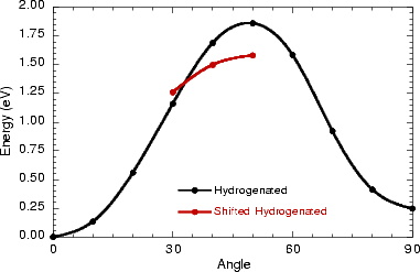
The energy barriers for the two processes are shown in Fig. 7.14, indicating clearly that the barrier to rotation in the shifted position is lower, if it can be reached. It is not surprising that the significant atomic rearrangement seen in the clean case cannot occur here, given the smaller number of degrees of freedom for the system. The barrier will lie between 1.6 and 1.9 eV, depending on how easy it is to reach the shifted position; however, these energies correspond to a temperature far higher than the highest temperature at which monohydride dimers are still seen on the surface (Owen 1996), making this rotation mode far less relevant overall than the clean rotation mode. As the post hoc GGA corrections are only likely to raise these barriers, they were not evaluated. The height of the barrier does explain why the only hydrogenated dimers imaged are non-epitaxial. The area where the rotation becomes interesting is in a dehydrogenation mechanism, which will be described in the next section.
The question of dehydrogenation of the non-epitaxial monohydride dimers which are formed is a very thorny one. The transition from hydrogenated dimers to clean dimers is seen at a temperature (420 K) which is much lower than either the lowest possible hydrogen desorption temperature (at least 700 K) or the temperature at which hydrogen becomes mobile on the clean surface (550 K) (Owen 1996). If the rotation mode for the hydrogenated dimer had included a transitional state which was entered with a barrier in the region of 1 to 1.5 eV, then that state could have played a part in the dehydrogenation mechanism (Owen 1996); however, as shown above, this is not the case. The situation which remains is that the rotation of the hydrogenated dimer probably plays a part in the dehydrogenation, but this is not well defined. To fully understand the mechanism would require a series of simulations for a diffusion event where a hydrogen atom moves off the ad-dimer onto the substrate, each with the dimer constrained at a different angle; this would have to be done using DFT, as tight binding cannot model the rotation, and would require a prohibitively large amount of computer time.
As a test of the feasibility of the diffusion off the dimer, a very simple calculation has been performed, using tight binding. In order to obtain the correct coordinates for the ad-dimer, the DFT positions for the 40o (symmetric) dimer were used, and all atoms apart from the hydrogen were constrained to remain in a fixed position. The hydrogen was forced to remain in vertical planes parallel to the substrate dimer rows, but was allowed to relax within those planes. The unit cell, as for the calculations above, was two dimer rows wide each of which was two dimers long, with five layers of silicon terminated as for all the DFT calculations. As with the diffusion calculations in Chapter 6, the hydrogen was only allowed to bond to the atoms where it started (the ad-dimer) and finished (a substrate dimer). The energy for this process is shown in Figure 7.15(a), and the pathway is indicated schematically in Fig. 7.15(b).
|
The barrier found, 1.4 eV, is extremely reasonable given the temperatures at which the dehydrogenation is seen to occur, and suggests that this may be the mechanism. As the cell is frozen, it is not clear whether the correction of Chapter 6 should be applied. However, this mechanism is not conclusive, and more comprehensive calculations using DFT, with full relaxation of the cell at each stage, would be required for certainty.
Experimental observations show that there is a large population of clean dimers over the trench after dosing with disilane above about 450 K. The next stage in growth requires these dimers to move, so that they can combine to form islands. The diffusion on top of the row has already been modelled (Yamasaki, Uda and Terakura 1996) and observed (Swartzentruber 1996) with reasonable agreement between the barriers. Recently dimers have been observed diffusing along the trench between dimer rows, with a measured barrier of 1.21±0.09 eV (Borovsky, Krueger and Ganz 1997). This diffusion has been modelled using LDA (Goringe and Bowler 1997), partially as an extension of the clean ad-dimer rotation mechanism, where the dimer moves along the row a short distance.
The single ad-dimer was placed between the dimer rows, over the trough in the non-epitaxial orientation (i.e. parallel to the underlying dimers), as shown schematically by a dotted line in Fig. 7.16b. In order to investigate all possible diffusion mechanisms, the energy surface (Figure 7.16a) was evaluated. For each point on the surface, the distance along the diffusion direction of the two atoms was fixed, and all other coordinates allowed to relax. The standard unit cell was used, which was the smallest cell which allowed no substrate dimer to be bonded to more than one ad-atom.
|
Line (AE) on Figure 7.16 represents the dimer diffusing intact and in its original configuration from a start site to an end site. This mode of diffusion gives a barrier of 1.8eV, which would be prohibitively high at temperatures below 800K; however, diffusion has been measured at temperatures as low as 450K (Borovsky, Krueger and Ganz 1997). There is an alternative path, shown as line (ABCDE) in Fig. 7.16(a), which gives a maximum barrier of 1.15 eV - in excellent agreement with the measured barrier of 1.21 eV.
This presents a method for diffusion (which is very similar to that predicted for diffusion on top of the dimer row (Yamasaki, Uda and Terakura 1996)) by break-up of the dimer (AB - barrier 1.15 eV), diffusion of one adatom (BC - barrier 0.36 eV), diffusion of the other (CD - barrier 0.58 eV) and reforming of the dimer (DE - barrier 0.23 eV). Since the energy barrier to the diffusion of adatoms (CD) is significantly lower than the initial breaking of the dimer (AB) (0.6 eV compared to 1.15 eV), it is likely that once a dimer breaks and the first adatom diffuses, the subsequent adatom diffusion will occur over a considerably shorter timescale. However, as the barrier is still considerably greater than kT, the second adatom will not always diffuse in the same direction as the first; it is equally likely that the first adatom will diffuse back to its original position. Indeed, given that the energy barrier (CD) is not significantly different from the adatom diffusion barrier in the absence of another adatom, it is almost equally likely that the second adatom will diffuse in the opposite direction.
|
The effect of this uncertainty in diffusion direction, and the typical distance the adatoms will move before the
dimer reforms, can be investigated with a simple statistical model of the diffusion of two particles. Assuming
diffusion of adatoms only along the trench, the state of the system can be described in terms of S(n,t), the
probability that the adatoms are separated by n dimers after t adatom diffusions have taken place, and D(d,t), the
probability that the centre of mass of the two adatoms has moved d/2 dimers after t adatom diffusions. At any
timestep one adatom diffuses at random, so the separation is equally likely to increase or decrease;
S(n,t) =  S(n - 1,t - 1) +
  S(n + 1,t - 1), and the centre of mass is equally likely to move in either direction;
D(d,t) =
S(n + 1,t - 1), and the centre of mass is equally likely to move in either direction;
D(d,t) =  D(d- 1,t- 1) +
  D(d + 1,t- 1). It is important to note that the S and D probability distributions are
independent of one another.
D(d + 1,t- 1). It is important to note that the S and D probability distributions are
independent of one another.
The initial boundary condition must now be added: at t = 0, one adatom has hopped by one dimer in a random
direction (S(1,0) = 1; D(1,0) = 0.5 and D(-1,0) = 0.5); and an additional condition that if the two adatoms come
back together they rebind and are removed from the system (S(1,t) =  S(2,t - 1)).
|
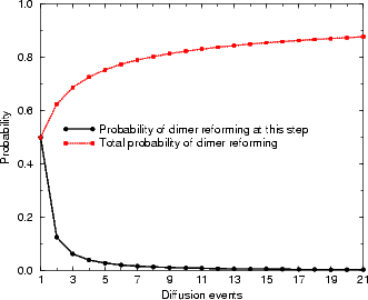
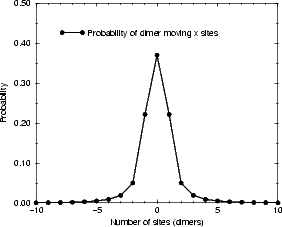
The evolution of these probabilities can be numerically calculated extremely easily. The probability at any
particular time step for reforming the dimer is then simply given by S(0,t), and the cumulative probability of
reforming the dimer by a given time is  nS(0,t). These are plotted in Figure 7.17. Of rather more interest is the
distance that the dimer has moved when it reforms; the distribution of dimer diffusion distances is plotted in Figure
7.18(a). Since a diffusion distance of zero represents an event which will not be observed, Figure 7.18(b) shows the
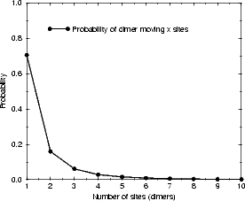
probability of diffusion distances given a non-zero distance. The majority (70%) of dimers in this model diffuse only
one unit of distance along the dimer row, and only 14% diffuse more than two. This diffusion mode gives a
barrier in extremely good agreement with experiment, and shows how the dimers which are formed
from the disilane fragments can diffuse. Borovsky, Krueger and Ganz (1997) also observed dimers
diffusing across dimer rows; this will be important in the formation of large islands at later stages of
growth.
nS(0,t). These are plotted in Figure 7.17. Of rather more interest is the
distance that the dimer has moved when it reforms; the distribution of dimer diffusion distances is plotted in Figure
7.18(a). Since a diffusion distance of zero represents an event which will not be observed, Figure 7.18(b) shows the
probability of diffusion distances given a non-zero distance. The majority (70%) of dimers in this model diffuse only
one unit of distance along the dimer row, and only 14% diffuse more than two. This diffusion mode gives a
barrier in extremely good agreement with experiment, and shows how the dimers which are formed
from the disilane fragments can diffuse. Borovsky, Krueger and Ganz (1997) also observed dimers
diffusing across dimer rows; this will be important in the formation of large islands at later stages of
growth.
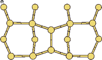
As has been mentioned above, clean dimers are formed on a Si(001) surface which has been dosed with disilane once the surface reaches 470K. These single epitaxial dimers amalgamate to form strings which grow anisotropically perpendicular to the substrate dimer rows (Boland 1991), by preferential adsorption of dimers at the B-type step edge at the end of the string (Pearson et al. 1996). The smallest length of epitaxial dimer string observed is three dimers; this is because it is the shortest length which allows rebonded step edges at each end. However, spontaneous formation of a three-dimer string from three isolated dimers is kinetically unlikely. The nucleation mechanism for these dimer strings is therefore unknown; this section describes a previously unknown feature on the Si(001) surface which may play a role in nucleation.
While this thesis is in the main about gas source epitaxial growth, there is enough contact with solid source (where no hydrogen is present) that it is worth reviewing the area. There has been considerable effort to determine the metastable structures that form as the nuclei of dimer strings in solid source MBE. The primary candidates seem to be diluted-dimer rows (Bedrossian 1995), and a pair of epitaxial dimers, one on top of the dimer row, and one in the adjacent trench, which will be notated as TR (Yamasaki, Uda and Terakura 1996). Diluted-dimer strings are ad-dimers which are parallel to the underlying dimer rows occupying only trench sites, and attract other adatoms to form long chains of trench dimers. These chains can then react with further adatoms to form epitaxial strings (Brocks and Kelly 1996) and can also form long chains of diluted dimers terminated in ad-dimers, as well as larger structures(van Dam et al. 1996). They are not usually seen in GSMBE (Wang, Bronikowski and Hamers 1994). The primary reason for this is likely to be that the hydrogenated ad-dimers which form during GSMBE do not attract SiH2 groups, and so long diluted-dimer chains do not form.
|
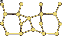
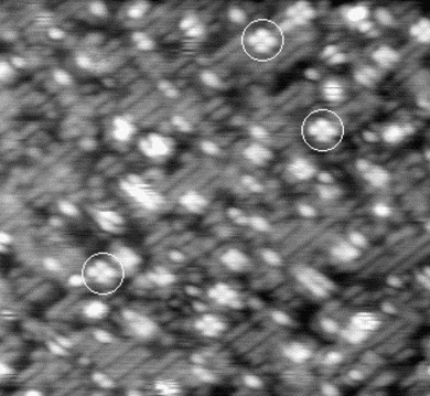
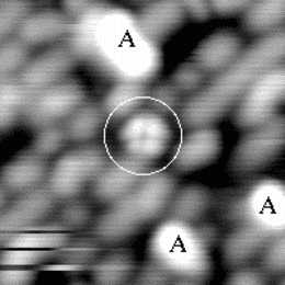
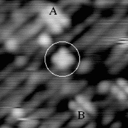
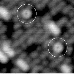
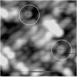
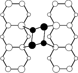
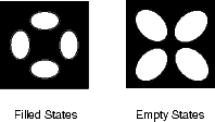
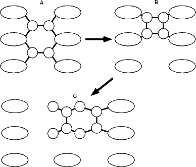
An image of the disilane-covered Si(001) surface at 550 K is shown in Fig. 7.19. This is an empty-states picture, in which the epitaxial dimer rows appear as two bright lines, with a dark node running down the middle. The background dimer rows appear grey; missing dimers and hydrogenated dimers appear black. The bright features are mostly clean rotated epitaxial dimers. The new feature is circled, and will be referred to as a square (Owen et al. 1996). It is situated between two dimer rows, and between two dimers (a schematic picture can be seen in Fig. 7.22a). These squares are seen after dosing with disilane at a substrate temperature above 400 K and appear to be stable up to 600 K. In filled states images (Fig. 7.20a), the square has two perpendicular nodes, running vertically and horizontally across the picture, which are at 45o to the underlying dimer rows. In empty states (Fig. 7.20b), the nodes are weak and are orientated parallel and perpendicular to the underlying dimers. By comparison, the epitaxial dimer row above it (A) has a much stronger node along its centre.
|
Images at different negative sample biases were taken in order to probe the electronic structure. A pair of pictures is shown in Fig. 7.21. As the sample bias is reduced, the contrast of the square changes relative to the background. At -1.7 V (a) the square is brighter than the background, but as the voltage is reduced to -1.0 V (b), it darkens until it is the same apparent level as the dimer rows. From such variable-voltage imaging, and careful comparison with other features on the surface, it is clear that the square is not a pair of epitaxial dimers. This is important, as a pair of epitaxial dimers situated on neighbouring dimer rows (e.g. the lower pair of dimers in Fig. 7.20(b)) looks similar to a square in empty states.
|
The structure initially conjectured, four silicon adatoms arranged over the trench between dimer rows in a square ring, proved to be unstable in tight-binding, distorting to form a rhombus-like structure with two opposite corners higher than the other two. This is shown schematically in Fig. 7.22(a). The unit cell used consisted of two standard unit cells side-by-side (making a unit cell two dimer rows wide, each six dimers long) with the square placed between the dimer rows. The STM images, however are symmetric. Modelling showed that the square structure can oscillate back and forth between two mirror images, so that the average, as seen by the STM, is a square. The energy barrier to this flipping was calculated to be 0.15eV. At room temperature it will flip millions of times a second, which will result in a symmetric, square appearance in the STM. A schematic average picture of the states which the STM will image is shown in Fig. 7.22(b).
The tight-binding calculations (using two standard unit cells side-by-side) indicated that this rhombus-like structure was 1.1 eV more stable than two isolated ad-dimers on the surface, in the lowest energy position. However, tight-binding underestimates the energy of the most stable ad-dimer, so this is likely to be an overestimate of the relative stability of the distorted square structure. When energy comparisons were made with two ad-dimers on the clean surface using LDA, the square was found to be 0.18 eV more stable than two isolated ad-dimers. These calculations were performed using the standard unit cell.
The alternative candidate for the most stable structure of four atoms, the TR structure modelled by Yamasaki, Uda and Terakura (1996), is found to be 0.0 eV more stable than two isolated ad-dimers by Brocks and Kelly (1996), 0.32 eV more stable by Yamasaki, Uda and Terakura (1996), and 0.49 eV more stable in these calculations. There is clearly some uncertainty about the stability of this structure, but the square feature is likely to be a little less stable than it. The square is, however, seen in great profusion in STM images (Owen et al. 1997a), suggesting that it is common, and that the formation pathway may well be kinetically easier for the square than for the TR structure. This will be dealt with in more detail in the next section.
|
There is some question as to whether the bonding of the square to one end of a dimer will cause the -bonds of
the dimers to be broken, thus giving a bright appearance to these dangling bonds, as is seen in the case of hydrogen
adsorbing on Si(001). However, in a manner similar to that shown above in section 7.1, the dangling bonds in
adjacent dimers bonded to the square transfer charge between themselves, and thus give an appearance
indistinguishable from the clean surface.
The stability and symmetrical appearance of the square have been explained by tight binding and LDA modelling. However, the behaviour with varying voltage (i.e. becoming darker relative to the dimer rows) is not - in fact, the opposite occurs, and the square becomes brighter in modelling. This suggests that, in the case of the square, the simple approach described in Chapter 1 and used in Chapter 4 is insufficient. The development of a better approximation must be left to others.
While the square feature is clearly a common and stable feature on the silicon surface during growth, it is not clear from the above investigation how it forms. Given that the dimer seems to be the basic unit of growth in GSMBE, there are two possible arrangements of dimers which would allow the square to form. These are shown schematically in Figure 7.23. The arrows which are on this diagram reflect the results of the modelling of these processes, which offer a path for the formation of the TR structure.
|
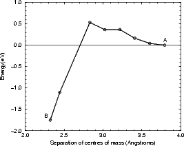
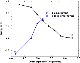
The formation of the square from two non-epitaxial row dimers was modelled using tight binding by fixing the separation of the centres of mass of the two dimers in the direction along the dimer rows (shown in Fig. 7.23) at each step on the pathway. The unit cell used was two dimer rows wide, each of which was four dimers long, with the usual termination. The energy barrier for the process is shown in Figure 7.24(a). The reaction proceeds from the right starting with two dimers (labelled A on the graph), as the distance between the dimers is being decreased, and reaches the square at a separation of 2.31 Å, labelled B. The net barrier is only 0.6 eV - extremely small, and indicative that the square will form from these two dimers very soon after they diffuse to adjacent sites at growth temperatures (the frequency of formation, assuming an attempt frequency of 1012 in an Arrhenius formula, is 6,000,000 times per second at 600K). The sharp drop at the left of the graph (leading to the formation of the square) is due to the strength of the bonds formed in the square. Given that clean dimers are formed from the disilane fragments deposited on the surface, and that there is a diffusion pathway along the trench between dimer rows, this pathway accounts for the large numbers of squares seen experimentally.
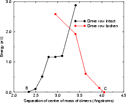
The next stage in the growth process is to transform the square into something else - either into a TR feature, as shown in the second part of Fig. 7.23, or as described in the next section. The TR is the most stable arrangement for four silicon atoms on the surface (Yamasaki, Uda and Terakura 1996, Owen et al. 1997) but is sterically unlikely to form from two ad-dimers, except from the cross-row diffusion mechanism. The decomposition of the square is a possible pathway for the formation of this feature (which would then have one “sticky” side for the formation of a small string of dimers). The reaction was modelled in tight binding by fixing the separation of the left and right pairs of atoms in the square in the direction perpendicular to the dimer rows (as shown in Fig. 7.23). The unit cell used was three dimer rows wide, each of which were four dimers long, and terminated in the usual manner. The energy for the reaction is shown in Fig. 7.24(b), and there are two parts to the graph depending on whether the substrate dimers are broken (labelled “dimer row broken” in red with squares) or intact (labelled “dimer row intact” in black with circles). The reaction starts from the square (labelled B) and proceeds to the right, arriving at the TR structure (labelled C). The barrier at the crossing point between these two curves is 2.1 eV, though this is, as in the next section, uncertain, and requires better modelling techniques on more powerful computers. The plateau on the “dimer row intact” curve represents the breaking of one of the square bonds, which gives a very soft vibrational mode to the system, allowing the flatness of the curve. However, the high barrier to formation may explains the relative infrequency of these features seen in experiment, though there may be a lower energy pathway based on the cross-row diffusion mode observed by Borovsky, Krueger and Ganz (1997).
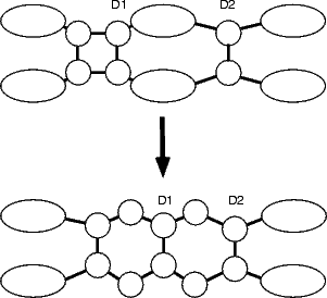
The square feature has the energetic advantage, in terms of growth, that it has two rebonded edges. If a trench dimer were to land next to either of these edges (as shown schematically in Figure 7.25(b)), it would be likely to stick (this position is at least 0.3 eV more stable than elsewhere on the surface in the same configuration) and then the whole ensemble could rearrange to give a string of three dimers (shown in the second part of Fig. 7.25(b)).
The reaction for formation of the string of three dimers was modelled in tight binding by constraining the centres of mass of the right-hand pair of atoms in a square (labelled as D1 in Fig. 7.25(b)) and an epitaxial dimer over the neighbouring trench (labelled as D2). The unit cell used was four dimer rows wide, each of which was four dimers long, and terminated in the usual manner. The energy for the reaction is shown in Figure 7.25(a). The plot starts on the right hand side, with the square and the dimer isolated (as shown at the top of Fig. 7.25(b) and labelled as B in (a)), and proceeds to the left. There are two curves, as was the case for the TR formation; the right hand one, referred to as “square intact” and labelled with circles in black, has the central substrate dimers and the square intact for most of its length, whereas the left hand one, referred to as “initial dimer formed” and labelled with squares in blue, has the left hand pair of square atoms forming the left-hand dimer of the string, the central substrate dimer broken and the middle pair of atoms of the square slowly forming the central dimer of the string. There must be a crossover point between these curves somewhere, but it is as yet not found. This puts the barrier at 1.5 eV as a minimum.
|
As with the formation of the TR, the use of the nudged elastic band method on a parallel computer would enable an accurate evaluation of this barrier. Nevertheless, it presents the energetics of the formation of a short string quite believably, and in good agreement with experiment: the value of 1.5 eV as a minimum is a little lower than would correspond to the temperature at which these strings are seen to form (Owen 1996); the barrier to adding a dimer onto a short string is 1.7 eV (Pearson et al. 1996). This evidence suggests that the model is reasonable, and that the nucleation process for dimer strings has been described.
Having spent the last 7 sections discussing the details of different reactions, it seems reasonable to step back and review the entire process. This also forms a useful link to the next section, which concerns the defects which form once islands start to meet.
|
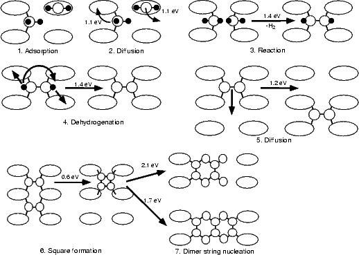
The entire pathway is summarised in Figure 7.26, which displays energy barriers for those processes modelled in this thesis. The sequence of events starts with the decomposition of disilane (in some manner) to yield SiH2 groups (1) and adsorbed hydrogen. The SiH2 groups diffuse around the surface (2) until two of them react to form a monohydride dimer (3). This then loses hydrogen (in a reaction involving partial rotation) to give a clean dimer (4). The clean dimer can diffuse around the surface (5), and two of them, once they are on adjacent sites, form a square(6). This then produces short strings of dimers, of length either two or three, by decomposition (7).
The behaviour once strings of dimers have formed is rather simple. These strings grow by addition at the ends, and by nucleation of a new string at the side(Pearson et al. 1996). The sequence of events will follow the pathway, resulting in short strings of dimers forming. Once this has occurred, these will grow into islands of new silicon in different places on the substrate. Unlike in SSMBE, where denuded zones are seen both above and below B-type step edges, these are not seen in GSMBE (Owen et al. 1997a,b). The reason for this is that the reactive rebonded B-type step edges are passivated with hydrogen, as discussed in Chapter 6. The next section covers what happens when two of these islands which are forming meet in anti-phase on the growing surface.
In the previous sections the atomistic reactions leading to the formation of short dimer strings on the clean surface have been discussed. After the formation of these strings, the development of the surface is merely a matter of formation of new dimers from newly deposited SiH2 groups and dimer diffusion. Once islands become large enough to start meeting as they grow in size, a new phenomenon occurs: the anti-phase boundary.
An anti-phase boundary (APB) can occur on the silicon surface during growth, due to the 2x1 (or higher) periodicity of the dimer reconstruction (Hamers, Köhler and Demuth 1989). An APB forms when the trenches between dimer rows in one island are in phase with the dimer rows on another island. It can serve as a nucleus for growth of a new layer of silicon (Bronikowski et al. 1993), and in gas source growth APBs are seen to nucleate islands when islands are not nucleating on clean terraces (Owen 1996). By analogy with steps on the silicon surface, there are two kinds of APB possible: one where the dimer rows are perpendicular to the APB (which will be referred to as a B-type APB, rather than AP2 as in Bronikowski et al. (1993)) and one where the dimer rows are parallel to the APB (the A-type APB). The B-type is considerably more interesting to the study of growth, as it is small enough in its most stable form to allow growth of a string of dimers along it, whereas the A-type APB is too wide. This is an experimental result - nucleation is seen to occur on B-type APBs but not on A-type.
|
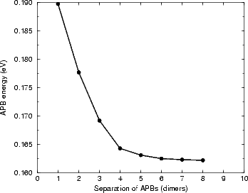
The interest in APBs occurs because they are high energy sites, and can therefore lower the barrier for growth of strings (a string on an APB will remove it, reducing the energy of the system). The nucleation of a string of dimers on an APB will concern us later in this section; first, the structure must be elucidated. As with the study of steps and kinks, it is important to determine the appropriate size of supercell to use for isolation of APBs. Figure 7.27 shows the energy per APB against separation for a unit cell containing two 0DV type-B APBs (the notation is explained in the next paragraph). The calculations were performed with TB, using cells one dimer row wide and of varying length (from two to sixteen dimers long) and terminated in the usual manner. The graph shows that almost complete convergence is attained at a separation of eight dimers, though convergence to meV accuracy is reached at a separation of five dimers. In the calculations of structures, the separation of eight dimers will be used, while in the larger unit cells used for kinking and dimer string nucleation calculations a separation of five dimers will be used. This is again a compromise between isolation and computational speed - the large cells have over 2,000 atoms in them.
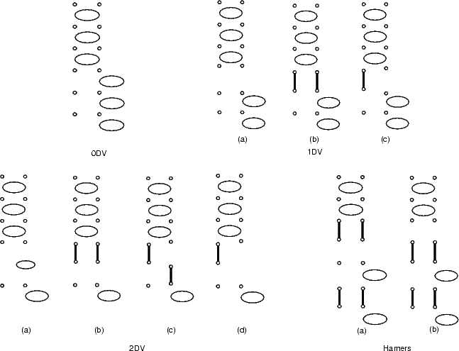
Now that isolation has been addressed, the most stable structure must be found. The APB could have dimers missing between the two different phases, and the structures considered have been named by analogy with the missing dimer defects (so that an APB with one dimer missing is a 1DV APB). In this work, structures with up to two dimers missing in the APB have been considered, as well as that proposed by Hamers, Köhler and Demuth (1989) from an experimental (STM) observation. Schematics of the structures with no dimers missing (0DV), one dimer missing (1DV), two dimers missing (2DV) and the experimentally observed (Hamers) are shown in Figure 7.28, and their energies relative to the most stable APB (the 0DV) are given in Table 7.3. These energies were found using TB, with unit cells sixteen dimers long and one dimer wide, terminated in the usual manner.
|
|
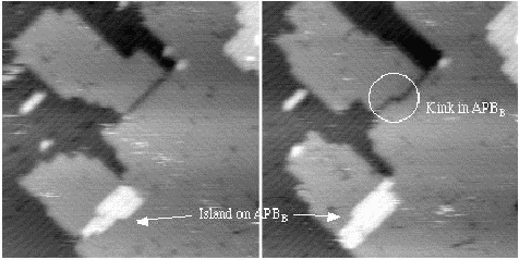
Figure 7.29 shows two STM images of the same area a short time apart. Both (a) and (b) show an APB in the lower left hand corner with an island nucleated on top of it. Fig. 7.29(b) shows a kink in an APB which has formed in the interval between the pictures. The kinking energy for a 0DV B-type APB has been modelled using TB in a unit cell ten dimer rows wide, with two APBs separated by five dimers each way. Forming a kink in the 0DV necessitates the removal of two atoms, but yields a kinking energy of 0.36 eV, which is not prohibitively high at 600 K. As all experimentally observed APBs are at least 1DVs, which will kink more easily (as no atoms must be removed, and there is more room for accomodation of strain), the structures found seem to be reasonable, and behave in a manner which does not contradict experimental results.
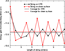
As mentioned above, the real interest in APBs is their ability to nucleate new islands of the second layer. Figure 7.30 shows the energy gained by adsorbing dimers onto the ends of strings of different lengths on a clean APB (a) and next to a string already on an APB (b). The energies were found with TB, using a unit cell ten dimers long and ten dimer rows wide, terminated in the usual manner. The differential energy is the important factor in dimer string growth. Fig. 7.30 (a) shows that the average energy gain for adding a dimer to a string on an APB is 0.1 eV higher than for adding to a string on a clean surface, and that the difference between adding to an even-numbered string and an odd-numbered string is much smaller than on the clean surface. On the clean surface, a string of an even-numbered length has one end unbonded and one rebonded, while an odd-numbered string has both ends rebonded and is more stable. On an APB there is no such effect, as the dimer rows either side are out of phase.
|
|
Indeed, it would seem that the energy for adding to both should be the same. However, as is clear from Fig. 7.30(a), the energy varies, and the reason why is illustrated in Figure 7.31. When there are an even number of dimers in the string, the twist forced by the underlying structure is the same at both ends of the string, and all the dimers twist in the same way. When there are an odd number of dimers in the string, however, the twist is in an opposite sense, and the central dimer is straight. This effect is enough to cause the slight variation of energy seen.
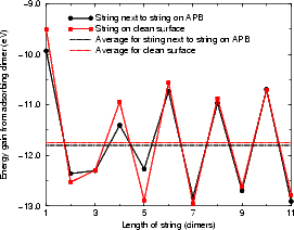
Fig. 7.30(b) shows the energy for adding a dimer to a string next to a string already on an APB. There is a small difference between this behaviour and that of adding to a string on a clean surface. The two results show why APBs are good nucleation sites for second layer islands, and indicate that a small amount of strain energy can have a large effect in growth processes.
Conclusions This chapter has presented the results for modelling all of the important processes involved in growth of the Si(001) surface from disilane, Si2H6. The pathway from the adsorbed fragments to clean dimers and small strings has been shown, and the nucleation of a second layer at high energy sites has been modelled. The results are in good agreement with experiment, and mean that, along with the experiments of Owen (1996), the atomistic aspects of the growth process on this surface have been comprehensively understood.