|
Every valley shall be exalted, and every mountain and hill shall be made low: and the crooked shall be made straight, and the rough places plain:
Ge/Si heteroepitaxial films are ideal for semiconductor manufacturers as they involve little change to existing fabrication technology, and yet allow the tuning of electronic structure and the extension of silicon devices to frequency regions where GaAs (or other expensive III-V materials) have been the only materials available. However, Ge on Si has a 4% lattice mismatch, and forms 3D islands when grown on a Si(001) substrate (an effect which is sometimes used deliberately - see Chapter 8). Ge also segregates to the surface when Si is grown over a Ge layer, leading to a diffuse interface (Fukatsu, Usami and Shiraki 1993). The use of gas-source MBE, where disilane and germane are used as the group IV source, rather than solid source MBE has been shown to reduce Ge segregation during growth of Si/SixGe1-x heterostructures (Ohtani et al. 1994). With these sources, hydrogen acts as a surfactant, improving surface quality. More common, however, is to use a large atom which will not easily incorporate in the growing substrate. Group V atoms such as As and Sb have been very popular for such applications (Copel et al. 1989; Fujita et al. 1990).
Sakamoto et al. (1994) showed that a surfactant layer of bismuth has two effects on SSMBE of Ge/Si heterostructures1, one beneficial and the other detrimental. A sandwiched structure was grown, alternating a thick layer of Si with a thin layer (4 ML) of Ge, four times and ended with a cap of Si. After the third layer of Ge, however, they deposited Bi, so that the growth of the final pair of layers before the cap (i.e. thick Si and thin Ge) were influenced by Bi. The structure was then investigated with high resolution TEM. The results of the first Ge layer were as expected - the Ge/Si interface was flat (suggesting that the Si surface on which the Ge grew was flat) but the Ge layer formed large islands, and the interface between the Ge and the next layer of Si was highly diffuse. Bi had a marked effect on this behaviour. It was deposited after the third layer of Ge, and had the immediate effect of making the new Si/Ge interface sharp, reducing the diffuseness seen before. It also prevented islanding of the Ge in the fourth layer; it had a detrimental effect, however, producing a far rougher Si layer (the fourth Si layer) and Ge/Si interface than had been seen before. Katayama et al. (1996) studied the effect of Sb and Bi on SSMBE of Ge on Si(001). An ion scattering technique was used to measure the mixing of Ge and Si, and the crystal perfection of the resulting layers. It was found that for increasing levels of surfactant, the intermixing was suppressed and the crystal quality improved. Sakamoto et al. (1993) used secondary ion mass spectroscopy (SIMS) to show that when Bi desorbs (above about 550o C), the amount of Bi left in the silicon is less than 5×10¹⁶ atoms cm-3 (the resolution limit of SIMS).
It is reasonably clear that Bi can act as a good surfactant for Ge/Si heterostructure growth. However, the behaviour of Bi on the Si(001) surface is still poorly understood, and so its surfactant action cannot be clearly understood. There have been several experimental studies, which have found variously (1x2) reconstructions (Noh et al. 1994; Franklin et al. 1995; Lyman et al. 1996; Kim et al. 1996; Qian et al. 1996), (2x2) reconstructions (Noh et al. 1994; Kim et al. 1996; Qian et al. 1996) and a strain-induced (2xn) reconstruction (Hanada and Kawai 1991; Park et al. 1994). The STM studies of Noh et al. (1994) and Park et al. (1994) show that at room temperature, Bi initially adsorbs as adatoms, sited between Si dimers on top of the rows, which then pair up to form dimers, perpendicular to the underlying Si dimers, and still on top of the dimer rows. These dimers would give rise to a (1x2) periodicity. The Bi ad-dimers align from row to row to give a (2x2) periodicity. There have been some calculations for Bi on Si(001) (Tang and Freeman 1994, Franklin et al. 1995, Qian et al. 1996) which used cluster calculations in LDA, with the DMOL code. These calculations do not use relativistic corrections, and (from the information available) do not perform relaxations on the cell, which makes their results a little dubious. It was found that the lowest energy state for Bi on the Si(001) surface is as a dimer perpendicular to the underlying dimers, but do not consider the two possible sites for it (i.e. over the trench between Si dimer rows as well as on top of the Si dimer rows). The (2x2) structure was found to be more stable than the (1x2) structure, in opposition to the experiments. A recent experiment using high resolution electron energy loss spectroscopy (HREELS) and ultraviolet photospectroscopy (UPS) (Gavioli, Betti and Mariani 1997) has found that the Bi dimers on the surface have a larger band gap than the Si dimers and a large density of states above the Fermi level, a point which will be important later.
The work in this thesis is part of a study of Bi on Si(001) with Kazushi Miki and James Owen. The work in Oxford involved STM, while SIMS and RHEED results have been obtained in Japan. The specific areas being studied were the minimum surface energy state for a Bi dimer on (or in) the Si(001) surface, and then two of the more unusual features generated during the STM study: large numbers of straight lines, running for hundreds of nanometers without kinking, which formed during annealing at the desorption temperature2, and a c(4x4) structure which formed if the surface was held close to the desorption temperature while adsorbing Bi. An interesting point which has emerged from the calculations (which is not surprising in view of its size) is that the Bi atoms are always either adsorbed on the surface or substituted for Si atoms in the surface: they are never in the second layer.
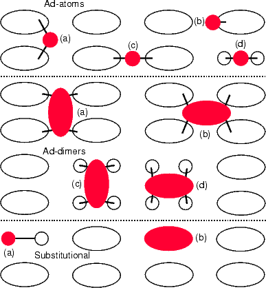
The first task in investigating the behaviour of bismuth on Si(001), and particularly in investigating the complex structures seen in STM, is to identify the lowest energy sites on the surface for Bi adatoms and dimers. This is a hard problem, as the usual procedure (to use a chemical potential of some sort for the Bi atoms) is not possible here, for there is no reservoir (for example, the bulk energy for silicon atoms; there is no SiBi alloy to use for this purpose). Accordingly, I have chosen to compare the excess surface energy (compared to a clean, perfect silicon surface) plus the Bi chemical potential per Bi atom. This is achieved by subtracting off the Si chemical potential multiplied by the number of silicon atoms from the energy, followed by the excess surface energy for a perfect silicon surface of the same area, and dividing by the number of bismuth atoms. The excess surface energy plus bismuth adsorption energy per Bi atom for a variety of structures (illustrated in Figure 5.1) is given in Table 5.1. All calculations were performed using TB and the parameterisation developed in Chapter 3, with two standard unit cells side-by-side, to create a unit cell six dimers long and two dimer rows wide.
|
|
With the dimers, an additional factor enters the question of stability: the Bi-Bi bond length. The most stable position is as a substitutional dimer ((a) in the substitutional section), followed by the epitaxial trench dimer ((a) in the ad-dimer section). It is perhaps not surprising that the substitutional dimer is more stable than any of the others, as it has the lowest excess surface energy. A comparison between the stabilities of the ad-dimers formed by bismuth and those formed by silicon is also interesting. The ordering for silicon has the two structures on top of the rows (i.e. in the same positions as (c) and (d) in Fig. 5.1) as the lowest in energy (and almost indistinguishable) and then the non-epitaxial trench dimer, with the epitaxial trench dimer being the worst. For bismuth, which is a much larger atom, the situation is almost completely reversed: the epitaxial dimer on top of the dimer row has broken the underlying bonds, leading to a much worse energy than the trench dimer, which is the only position where there is enough room for the Si-Bi bonds to relax fully.
The normally observed configuration for Bi (in STM) is as a dimer; it is a useful confirmation of the Si-Bi parameterisation developed that the dimer is found to be the lowest energy conformation; however, the most commonly observed location for the dimer, over the Si dimer rows, is calculated to be much higher in energy than the dimer over the trench between the Si dimer rows. In view of the accurate predictions later in the chapter, it may well be that this disparity is due to kinetics. As the adatoms are observed to adsorb on top of the rows, the pathway to formation of ad-dimers on top of the rows may well be enhanced. The low-energy positions of these dimers (substitutional and in the epitaxial position over the trench between dimer rows) will be important in the coming sections.
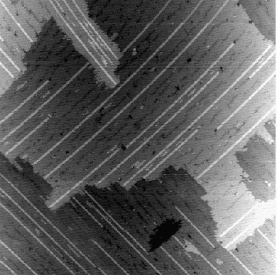
The first of the interesting features which will be investigated is perhaps the most startling, and is potentially useful as a basis for quantum wires. If bismuth is adsorbed onto silicon well below the desorption temperature, the standard (2xn) structure is formed. When this sample is heated to around the desorption temperature (545oC), and annealed there, the surface undergoes a radical change. Large, flat terraces of silicon are formed (indicating the efficacy of Bi as a surfactant) which have lines running across them, perpendicular to the dimer rows. These lines are perfectly straight and run for hundreds of nanometres, probably making them the straightest lines in the world. An example is shown in Figure 5.2
|
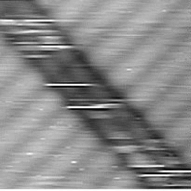
These lines take up the equivalent of three dimers in the Si(001) surface, and have an internal structure which shows two features, in phase with the dimer rows, and brighter than them at high bias, though darker than them at low voltage. In line with the principles of interpretation discussed in Chapter 1, this suggests that they are at the same height as the silicon dimers, but with a larger band gap. A close up of the line is shown in Figure 5.3.
There are two questions to ask about these lines, to which atomistic modelling should be able to provide pointers, if not answers. Firstly, why are they so straight ? Secondly, how do they form ? The answers to both of these questions are intimately concerned with the structure of the lines, which therefore becomes of paramount importance.
|
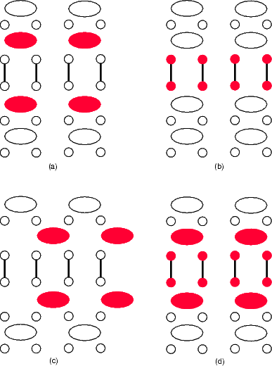
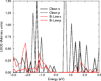
There are various structures which would match the description given above, the most plausible of which are shown in Figure 5.4. The energies for these structures (as in the first section, an excess surface energy plus a Bi adsorption energy, though this time per dimer rather than per atom) are shown in Table 5.2, calculated using TB and a unit cell ten dimers long and one dimer wide with the standard termination. The link between all of these structures is the substitution of two dimers and a missing dimer defect for three silicon dimers; with Bi involved, the energetics of the 1DV are more favourable (due to the longer bond lengths) and the dimers will be closer together than with pure silicon. The two most stable structures ((a) and (c)) have bismuth in the top layer, not in the second; the out-of-phase structure, (c), is unlikely to be a candidate, as it would appear out-of-phase in STM images, and this leaves the first structure, (a). LDOS calculations for the Bi dimer, compared to a clean Si dimer, in structure (a), are shown in Figure 5.5 and indicate a wider band gap in keeping with STM and UPS observations. The energetic stability and close correspondence with the STM images suggest that this structure is indeed what is seen as the lines. These lines should probably be referred to as quantum anti-wires, due to their band gap. It is possible, however, that they could be used as the substrate for quantum wires. More experiments will be needed to explore this exciting possibility.
|
|
Having identified the structure of the line, the questions of kinking and growth can be addressed. The most
obvious cause for the straightness of the lines, particularly at the high temperatures used, would be thermodynamic
- the kinked structure may have an energy which is so much higher than the unkinked structure that the population
of the kinked state is nearly zero. The simplest test of this is to take a unit cell, and calculate the increase in energy
after forcing it to kink. This kind of approach was extremely successful in identifying the GaAs(001)- 2(2x4)
reconstruction (Avery et al. 1996), where similarly straight dimer rows are seen. However, when it is done for the
line structure identified (using TB and a unit cell ten dimers long and six dimer rows wide with the usual
termination), the increase in energy due to the kink is far too small to account for the straightness of the
lines (less than 0.1 eV per kink). The reason for this seems to be the almost complete isolation of the
dimer rows - there is only a third layer atom connecting the two, and this is hardly strained by the
kink3.
The possibility that there is a long, conjugated bond along the line (which would give an interaction
between rows) is ruled out on two counts: firstly, the STM images, which show a clear gap between
dimer rows; secondly, modelling of this structure (where the Bi atoms in the dimers would be much
more evenly spaced) which proves to be unstable. Clearly, some other mechanism is at work. The
first clue can be found it Table 5.2, where it can be seen that the structure with the Bi atoms in the
second layer is disastrously poor in energy - at least 5 eV per dimer worse than the structures where Bi
is in the upper layer only. This suggests (not surprisingly, given its size) that the energetic cost of
placing a Bi atom in the second layer is prohibitively high, and provides a clue to the straightness of the
lines. The normal mode for diffusion of defects (Watanabe and Ichikawa 1997; Yamasaki, Uda and
Terakura 1996), where one dimer is displaced into the second layer, while two second layer atoms rise
to form a new dimer (a process which has a barrier of 1.6 eV (Kitamura, Lagally and Webb 1993;
Yamasaki, Uda and Terakura 1996)), is barred, as the Bi dimers cannot go into the second layer. So,
if the lines were to form straight, they would remain straight. Therefore the formation mechanism,
which must account for the straightness of the lines, must be elucidated. The experimental evidence is
that there are different areas where these lines form: in the terraces; as islands on the terraces or
jutting out from step edges (peninsulas); and in the terraces, but a layer lower than the surrounding
silicon (inlets). The first two of these are shown in Fig. 5.2, while the third is sufficiently rare that it
will be discounted, except as further evidence that Bi cannot enter the second layer of the growing
crystal.
2(2x4)
reconstruction (Avery et al. 1996), where similarly straight dimer rows are seen. However, when it is done for the
line structure identified (using TB and a unit cell ten dimers long and six dimer rows wide with the usual
termination), the increase in energy due to the kink is far too small to account for the straightness of the
lines (less than 0.1 eV per kink). The reason for this seems to be the almost complete isolation of the
dimer rows - there is only a third layer atom connecting the two, and this is hardly strained by the
kink3.
The possibility that there is a long, conjugated bond along the line (which would give an interaction
between rows) is ruled out on two counts: firstly, the STM images, which show a clear gap between
dimer rows; secondly, modelling of this structure (where the Bi atoms in the dimers would be much
more evenly spaced) which proves to be unstable. Clearly, some other mechanism is at work. The
first clue can be found it Table 5.2, where it can be seen that the structure with the Bi atoms in the
second layer is disastrously poor in energy - at least 5 eV per dimer worse than the structures where Bi
is in the upper layer only. This suggests (not surprisingly, given its size) that the energetic cost of
placing a Bi atom in the second layer is prohibitively high, and provides a clue to the straightness of the
lines. The normal mode for diffusion of defects (Watanabe and Ichikawa 1997; Yamasaki, Uda and
Terakura 1996), where one dimer is displaced into the second layer, while two second layer atoms rise
to form a new dimer (a process which has a barrier of 1.6 eV (Kitamura, Lagally and Webb 1993;
Yamasaki, Uda and Terakura 1996)), is barred, as the Bi dimers cannot go into the second layer. So,
if the lines were to form straight, they would remain straight. Therefore the formation mechanism,
which must account for the straightness of the lines, must be elucidated. The experimental evidence is
that there are different areas where these lines form: in the terraces; as islands on the terraces or
jutting out from step edges (peninsulas); and in the terraces, but a layer lower than the surrounding
silicon (inlets). The first two of these are shown in Fig. 5.2, while the third is sufficiently rare that it
will be discounted, except as further evidence that Bi cannot enter the second layer of the growing
crystal.
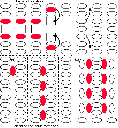
Two possible modes of formation have been modelled, which are shown by two kinds of line (equivalent in structure, though not in location): the first kind grows in the terrace, while the second kind either grows out from a step (continuing a line in the terrace) or forms on the terrace, surrounding itself with a small, ragged island of silicon. While both of these growth modes are illustrated in Figure 5.6, they will be dealt with separately.
|
Firstly, the growth in the terrace will be examined. All calculations were performed using TB and a unit cell ten dimers long, and between six and eight dimer rows wide (depending on the termination of the line described below). In Figure 5.2, it is reasonably clear that many lines end in a (roughly) square defect. This is (by extension of the notation in Chapter 4) a pair of 3DVs, and it is likely that these are involved in the growth. What must be calculated to elucidate the mechanism is the energetics of the termination of a short segment of line. The unit cell used for the different calculations had 3 dimer rows containing Bi (as shown in the upper part of Fig. 5.6), possibly some termination, and 3 dimer rows of Si to isolate the termination. These show that, while a single 3DV is less stable than no termination (by 0.65 eV), two 3DVs are more stable than no termination (by 0.2 eV); this explains the STM images, and gives a strong indication of the growth mode. A line is most stable if it is terminated in a pair of 3DVs rather than in perfect Si dimer rows or a single 3DV, and at the temperatures used in the experiments (about 800 K) the Si will be sufficiently mobile for these to form. It is energetically more favourable for Bi dimers to be in the surface than on it (as described in the previous section), and so any Bi dimers on the surface will move to fill in the 3DV, creating a new segment of line, terminated in a single 3DV. More silicon will move out of the surface (relocating to step edges or islands on the surface), creating a new stable pair of 3DVs. The mechanism repeats while Bi is available on the surface, and is shown schematically in the upper half of Fig. 5.6. While growth of these lines was observed in STM movies, it proceeded too fast to allow confirmation of this growth mode. The only drawback to this mechanism is that a pair of 3DVs offset from the Bi line by one dimer is calculated to be as stable as a pair of 3DVs in line. However, this configuration is never seen in experiment. It may be that the relative stability of the offset cell was due to the unit cell being too small; the size used was nearly at the limit of available computing power and memory. The experimental evidence is a good start, and indicates that this mechanism is certainly plausible.
The growth of peninsulas from step edges, and line segments on top of terraces (as seen in Fig. 5.2), also demands an explanation. The proposed process is shown schematically in the lower half of Fig. 5.6. (The calculations used TB, and a unit cell made up of two standard unit cells side-by-side, making a unit cell two dimer rows wide and six dimers long.) It has already been established that the lowest energy position for a Bi dimer is over the trench between dimer rows in the epitaxial position (Fig. 5.6(a)). This line can extend along the trench (and is 0.2 eV more stable than an isolated Bi dimer) and does not kink (the energy for two dimers, one over the trench and one on the dimer row, is 0.55 eV worse than two dimers over the trench), as shown in Fig. 5.6(b). Once a line is established, it is 0.2 eV better for it to have two silicon dimers next to it, building a small island; it is, however, then 0.2 eV better to add a second Bi dimer, epitaxially oriented, over the neighbouring trench than to continue the silicon building. This then has silicon added next to it, building a small island which contains a line (Fig. 5.6(c)). The only difference which would be seen at a step edge would be that Bi dimers arriving initially would be lining up with the dimers in the line in the upper terrace. The exact details of formation after (b) are unclear, and might vary from island to island. Unfortunately, only the presence, and not the growth, of these features has been observed in STM. It is also conceivable that they could form as a result of etching during annealing.
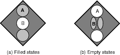
It has recently been found that a c(4x4) reconstruction can be induced on the Si(001) surface; this has been observed after the adsorption of boron (Wang, Hamers and Kaxiras 1995), trimethyl gallium (Nörenberg, Bowler and Briggs 1997), bismuth (Miki et al. 1997), hydrogen (Uhrberg et al. 1992) and silicon (Zhang, Kulakov and Bullemer 1996). At first glance, these all have certain similar features in STM: in filled states, bright blobs every four dimers, with an offset between dimer rows; in empty states, the bright blobs are every other dimer, and there is no offset between dimer rows, and at higher bias, there is more detail visible - between alternate bright blobs (i.e. every four dimers), there are split features (similar to the empty states Si dimer in appearance). These features are illustrated schematically in Figure 5.7. The apparent size and contrast of these features vary between different experiments, though there is some consistency: the features labelled A in Fig. 5.7 are smaller in filled states and larger in empty states than those labelled B for the group III and V cases, whereas in the clean Si case A and B are more uniform.
|
There is something peculiar occurring in these experiments, for all the different preparation modes give relatively similar STM images. There has been a recent suggestion (Kazushi Miki, Private Communication) that all of these reconstructions are the same, being induced by small amounts of an adsorbate which strains the surface and stabilises a clean Si c(4x4) reconstruction, such as that suggested by Uhrberg et al. (1992). This theory is based on SIMS experiments which show the presence of about 1% of carbon in the top few monolayers. With the clean Si c(4x4) results, this explanation seems not unlikely; however, with the group III and V compounds there is good evidence that the adsorbate is involved in large amounts in the reconstruction. Wang, Hamers and Kaxiras (1995) used Auger measurements to confirm that they had up to half a monolayer of boron on the surface in their images, which indicates strongly that boron is involved in the reconstruction; they also found an increase in the amount of the reconstruction with increased dose. Nörenberg, Bowler and Briggs (1997) also found an increase in the amount of c(4x4) with Ga exposure, but were unable to measure the Ga coverage in Auger. The shape of the patches which form in these and in the Bi results (Miki et al. 1997) are highly ragged, and often form at step edges, which suggest a reconstruction based on embedding rather than small amounts of strain. With these results in mind, an identification based on the presence, rather than the absence, of Bi will be made. However, there are some intriguing unexplained results still in the literature, mainly concerned with clean Si, which cannot be solved here. It may well be that the explanation of Miki is correct for these results.
|
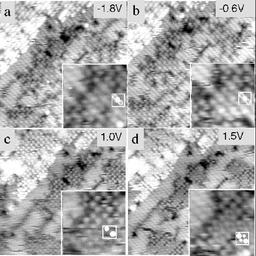
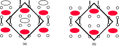
The c(4x4) structure forms when bismuth is deposited while the clean Si(001) surface is being annealed at about 570oC. An example is shown in Figure 5.8, which shows the reconstruction at different bias voltages, with magnifications and schematics clarifying the structures. The essential features to be noted are: in filled states, the most prominent feature, which occurs every fourth dimer, forms squares at 45o to the dimer rows (this feature is shown with a white dot between two grey dots in the inset in Fig. 5.8(a)) and is surrounded by two grey dots; in empty states, at low bias voltage (i.e. near the Fermi level), a square pattern of prominent features is visible which is smaller and not rotated with respect to the dimer rows; at higher bias voltage, a faint double feature becomes visible between every fourth brighter blob, which corresponds to the prominent features in filled states (this is illustrated schematically in the inset of Fig. 5.8(d)).
There are two important observations which help to identify the structure of this phase: firstly, that a silicon dimer appears as a dot in filled states and as a double feature in empty states; secondly that HREELS of Bi dimers (Gavioli, Betti and Mariani 1997) shows that on the Si(001) surface, they have a large density of states above the Fermi level - significantly larger than the clean Si(001) surface. These two facts suggest a structure, schematically illustrated in Figure 5.9(a): the prominent feature in filled states, which splits into two blobs in empty states, is a silicon dimer, while the prominent feature in empty states, which is darker in filled states, is a bismuth dimer. Another possible unit cell, where the Si dimer is missing (which is seen occasionally in large patches of the reconstruction) is shown in Fig. 5.9(b).
|
The so-called alpha structure, which forms the majority of the reconstruction, shows all the right features to match with the STM images, and has a very reasonable energy - 6.5 eV per Bi dimer (found using TB and a unit cell four dimers long and two dimer rows wide with the usual termination). The beta structure is slightly less stable, which might account for the lower proportion seen. As seen in the case of the lines, the possibility of the Bi being in the second layer is ruled out by the energetic cost - 5 eV per Bi dimer. There is no experimental evidence for the growth of this mode, and there are few theoretical clues. This will have to be left to future work.
Conclusions This chapter has covered some of the most exciting areas in silicon surface studies - adsorption, surfactants, controversial reconstructions and the possibility of quantum wires. The parameterisation developed in Chapter 3 has generated results which are in reasonable agreement with experimental observations. Models for the Bi line structure and growth and the Bi c(4x4) reconstruction have been proposed which fit all available experimental data.