The life so short, the craft so long to learn
Gas-source growth (so called because the silicon source is a gas rather than silicon atoms evaporated from a Knudsen cell, as is the case for solid source growth) involves the family of silane gases (SiH4, Si2H6 and so on) which are the silicon analogue of the alkanes. Traditionally, growth of silicon and silicon/germanium multilayers has been performed using solid source growth; recently, gas source growth has been proposed as an alternative, mainly for cleanliness and doping reasons. Solid source molecular beam epitaxy (SSMBE) uses cells at up to 2000oC, which introduces significant contamination problems, and the necessary substrate temperatures can cause dopant and germanium segregation - these problems are avoided by gas source MBE (GSMBE), which uses room temperature gas, and lower substrate temperatures. The passivating and surfactant effects of the hydrogen on the substrate convey additional benefits. While industrial processes use silane itself (due mainly to the lower cost of production) academic investigations tend to use disilane (Si2H6), which breaks up more easily, allowing growth at lower temperatures1, and without the use of an activator such as chlorine. However, this difference should result in little change to the results found in this work.
The study of growth from these gaseous hydride precursors has a number of interesting and important facets. The differences between it and solid source growth are extremely interesting, and are due both to the hydrogen present, and the different pathways to formation of clean silicon dimers, as explained in Chapter 7. The extension of GSMBE to SiGe alloys is extremely exciting for possible future applications in the electronics industry. At the most basic level, the study is interesting because the key atomic reactions involved in the growth are not understood.
The work which is presented in this thesis involves the computational modelling of the (001) surface of silicon (the face most commonly used for industrial growth and device fabrication), the behaviour of two relevant elements on the surface (hydrogen, which comes from the gas itself, and bismuth, which is another possible surfactant though is more likely to be used in SSMBE than GSMBE), and the reactions which occur in the growth of a new layer of silicon from disilane. This allows the entire pathway to be understood, which will have implications for larger-scale models of growth, and hence actual industrial processes. There is also an investigation of the best tight binding method for modelling these processes, and a description of the development of appropriate parameterisations to allow this.
One of the key ingredients for the success of the theoretical study was a very close interaction with experiments. This interaction will be expounded upon later in the introduction, and it has been my aim, where possible, throughout the thesis to highlight those areas which would have been impossible without interaction - both from the theoretical side, and the experimental side. James Owen has already been acknowledged as a very important co-worker, and his thesis (Owen 1996) forms an important companion volume to this, detailing the experiments more fully than is possible here.
At the recent inauguration of the Convex Exemplar in the Materials Modelling Laboratory (MML), I was talking to a director of a medium sized industrial firm, which specialises in alloys. He was telling me that, in the last ten years, materials modelling has gone from being “worse than useless” in the prediction of the properties of new materials (specifically, heats of formation were a factor of ten out) to actually producing useful predictions today. It is the ability to model materials at the level of a few atoms sufficiently accurately that macroscopic properties can be predicted that is the eventual goal of all materials scientists. The motto of the MML is “linking the length scales” - that is, understanding how to relate results using one technique to those from another. One of the best examples of this is looking at how a material cracks - at the tip of the crack, individual bonds are breaking, and the quantum mechanical description of these bonds must be correct; a little further away, two new surfaces are forming, and the behaviour of the atoms must be accounted for; as the crack broadens, the microstructure of the material becomes important; and at the largest scales, continuum elasticity theory can predict strain and heat dissipation. At each of these levels, the modelling method described is sufficiently accurate for the results required, and allows simulations to take place in a reasonable amount of time.
The length scales covered range from Ångströms to metres, and the time scales from femtoseconds to minutes, or even hours. The work here covers only scales from Ångströms up to a few tens of nanometres, and time scales from femtoseconds to a few tenths of a picosecond. However, there is a very high possibility that the reaction barriers which have been found herein will be used in a kinetic Monte Carlo model, which should enable simulations to cover up to a micron of growth on a cell 100 × 100 Ångströms, covering an hour of simulated time. The technique to be used has already been proven by Battaile, Srolovitz and Butler (1997) for diamond growth. The eventual aim of the whole project is to produce predictions of layers grown which will be sufficiently accurate to enable planning before growth commences in a reactor.
While I am not an experimentalist per se, I have had to learn a fair amount about various different experimental techniques, their limitations, and (most importantly) what they can and cannot measure. The work which I have performed over the last three years has revolved around the real space data which Scanning Tunneling Microscopy (STM) can give, though other techniques have been relevant, and certainly results from the literature must be born in mind. I shall therefore give a brief description of the principles behind the various relevant surface science techniques and their areas of applicability.
Since the 1960s, surface science has burgeoned as a discipline in its own right, as the development of ultra-high vacuum (UHV) systems, and computers and codes, have enabled rigorous understanding of the relevant processes (Zangwill 1988). Since the invention of the STM (Binnig et al. 1982), an atomic-scale, real space understanding has become possible. The importance of UHV as a means of preparing a “clean” surface, as opposed to a “real” surface (Many, Goldstein and Grover 1965) cannot be underestimated; this ability to image atomic processes has brought about the work in this thesis.
The scanning tunneling microscope works in a very simple way: a sharp, conducting tip is brought to within a few Ångströms of a conducting surface, and a voltage is applied between them. When the tip and surface are brought together, electrons can tunnel through the barrier (caused by the insulating vacuum gap) in a well-known quantum mechanical effect. By applying a voltage between the two, the tunneling in one direction is enhanced over the tunneling in the other, giving rise to a current. The magnitude of the current is strongly related to the size of the gap (from a simple treatment, it appears to be exponential) and also to the electronic properties of the surface. If the tip is scanned over the surface, a map of the topography can be built up. The most common mode of imaging, one used for all pictures in this thesis, is known as constant current; a simple feedback mechanism is used to adjust the height of the tip, so that the current flowing remains constant, and the height of the tip as it scans is displayed. This is suitable for high magnification work at reasonable temperatures. If images at high temperature (over 700K) or images of very rough surfaces are desired, then the tip must be scanned at constant height, and a display based on the logarithm of the current is produced.
The STM cannot give any chemical information, except in as much as the electronic behaviour of different species may give rise to a variation in contrast. One valuable tool for obtaining broadly averaged chemical information is Auger Electron Spectroscopy (AES). In this technique, a beam of high energy electons (over 1 keV) is directed at the sample, and the back-scattered electron spectrum, N(E), is collected. Taking the derivative of this spectrum, dN(E)/dE, magnifies small oscillations in the signal due to secondary electrons. If an incoming electron collides with an atom in the solid, and ionises a 1s electron, then a hole in the 1s shell will result. A 2s electron can drop down to fill this, and the transition energy can eject a second, Auger electron from the 2p shell, which has an energy characteristic of the transitions involved and the atom in which it occurred. These have been tabulated for all of the atoms in the periodic table except for hydrogen and helium; by measuring the relative strengths of the different peaks in an Auger spectrum, a measure of the proportions of different elements can be built up. A related procedure, X-ray photoemission spectroscopy (XPS), again takes advantage of the core-hole binding energies. The sample is illuminated with a source of monochromatic X-rays, and the spectrum of emitted electrons displays peaks at kinetic energies characteristic of elements in particular environments. Both of these techniques are sensitive to about 1% of surface coverage.
An alternative, though destructive, way of obtaining chemical composition is to remove the top few layers and perform mass spectroscopy on them. Secondary Ion Mass Spectroscopy (SIMS) does just this, by bombarding the surface with a beam of ions or atoms with high energies (greater than 1 keV). Atoms, or clusters of atoms, which are sputtered off are then sent into a mass spectrometer, yielding information at the level of 10-6 of a monolayer - far more sensitive than AES or XPS.
Crystal structure can be very important, particularly during growth, and there are two common ways of monitoring this. Low energy electron diffraction (LEED) fires electrons with energies in the range of 20-500 eV at the surface, and collects the elastically back-scattered electrons. These then form a Fraunhofer diffraction pattern which is the Fourier transform of the surface atomic arrangement. A sharp pattern (shown by crisp spots) implies a well-ordered substrate, whereas a diffuse one will indicate a basic structure, but some disorder; it is worth noting that the symmetry can be lower than that implied on the LEED screen. A related technique, that of reflection high energy electron diffraction (RHEED), is used most often to monitor crystal growth. A beam of high energy electrons is fired at the surface at an extreme grazing incidence angle. Those electrons which are scattered through only a few degrees will sample the first 1-2 atomic layers, and no more. If the specular beam is monitored during a growth experiment, then regular oscillations are seen, corresponding to smooth and rough surfaces, which allows layer-by-layer growth to be monitored.
There are many experimental techniques which are relevant to this area, and I have given a brief introduction to the most important. However, there is more to the experimental-theoretical interaction than simply taking experimental results and modelling them, or vice versa. If the interaction proceeds on a day-to-day basis, as was possible in the department for myself and James Owen, then a mutual trust and respect is built up, and the level of interaction deepens. Ideas can form over coffee (or beer !) which require joint expertise; a deeper understanding results on both sides when explanations must be made; a synergy occurs which results in new understandings, and a feedback mechanism comes into play: as results are discussed, new experiments or calculations come to light, which then feed back into the discussion. In this way, new pathways have been discovered - for instance, the square feature which will be described in Chapter 7 would never have been found without the interaction, and the formation of dimer strings from this would have remained a mystery.
When STM first appeared, there appeared to be little problem interpreting the images. Tersoff and Hamann (1983) produced a theory of STM current flow which worked well for metals though not for semiconductors; however, as time has gone on, the question of how easy it is to obtain reliable, quantitative interpretations of STM images has become far more vexed. Even in the (apparently) simple system of a metal surface interacting with a metal tip, there are many areas of interest, in which recent progress has been made (Clarke et al. 1996). As well as the question of tip-sample interactions, there is the question of simulated images, and the effect of the electric field on the images. Issues related to some of these areas have been addressed by Ness and Fisher (1997) and Fisher, Blöchl and Briggs (1997).
However, tip-sample interaction and simulating images, while fascinating, are not the concern of this thesis. The main drive of the thesis is surface structure and surface reactions: how they can be modelled, and how they can be related to the available experimental data. As the most readily available, and most appropriate, data is from the STM in Oxford, a means of interpreting the images and relating them to calculations has been developed. The guiding principles used are listed below.
These principles have performed well in general, allowing a fruitful interaction to develop. For those interested in the questions discussed above, it could be interesting to examine where, and why, these principles break down; however, this must be left to others.
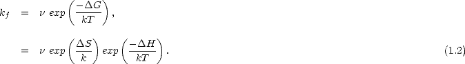
Much of this thesis is concerned with the calculation of reaction barriers and their relationship to the experimental temperatures at which certain process are seen to occur. The formal theory of kinetics states that a reaction rate will occur as (Christian 1965):
|
| (1.1) |
 is the vibrational partition function of the reactants and
  G is the free energy difference between the
start point and the transition state. There are two key assumptions which are made in the derivation of this
formula (see Christian 1965 and Glasstone, Laidler and Eyring 1941 for further discussion), which are
that:
G is the free energy difference between the
start point and the transition state. There are two key assumptions which are made in the derivation of this
formula (see Christian 1965 and Glasstone, Laidler and Eyring 1941 for further discussion), which are
that:
Equation 1.1 can be rewritten, using the fact that G = H -TS (where H is the internal energy and S is
the entropy of the system), and factorising the first term into a characteristic frequency of vibration,  ,
,
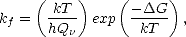
This theory was further developed and applied to solid-state reactions by Vineyard (1957), who showed that Eq.(1.2) could be further simplified to give:
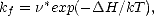
| (1.3) |
* = exp(S/k), and that the entropy could be written in terms of the frequencies of the normal modes
of the system. Vineyard made the further assumption that the motions of the atoms in the system both at the start
point and at the transition state can be treated as small, harmonic oscillations when deriving this
theory.
The formal theory as presented above has one drawback, as far as the calculation of reaction rates is concerned:
it is extremely difficult to calculate a frequency, *, for use in the formula. It is also important to realise that these
frequencies are temperature dependent.
When reaction rates have been calculated for comparison with experiment, or equivalently, when a barrier has been inferred from a reaction rate which has been measured, various assumptions have been made:
*, and uses Eq.(1.3) for comparisons).
The reader should be aware that the inaccuracies inherent in the approach given above will be quoted as an error; for instance, at about 600K, the use of a frequency of 1013 rather than 1014 will change the barrier calculated by about 0.1 eV.
The reader may find it helpful at this point to have an overview of the thesis, so that he or she can gain a broad view of the material involved. One of the more pleasurable aspects of writing this thesis has been the drawing together of three years’ work into a coherent whole, and I would like to pass this feeling on to the reader. This thesis has two main themes: the application of tight binding and density functional theory to the problem of growth of silicon from disilane (and related topics); and the importance of experimental-theoretical interaction. Without the experimental work which has been progressing during my time (and in particular without James Owen) very little of what is in this thesis would have happened.
The thesis starts with a description of the theory which underlies the techniques I have used. Density functional theory is described, along with several of the areas which I feel that it is important to understand before DFT results can be relied upon. The basis for tight binding is then discussed, and four of the recent linear scaling methods are presented in some detail; this area is a particular strength in Oxford, and that expertise has been exploited. Chapter 3 is rather more involved in the nitty gritty details of modelling, and starts with a comparison of the four linear scaling methods available in the MML. The systems examined are biased towards those relevant for this thesis (i.e. semiconductors and their surfaces). The chapter ends by describing three tight binding parameterisations which I have developed for this work.
Before any problems of reactions on surfaces can be considered, the clean surface and its defects must be understood. Chapter 4 presents the silicon (001) surface and the structure of the most common defect. A discussion of steps and their kinking behaviour rounds it off. Chapter 5 considers a new surfactant, bismuth (a horrible element to model), and presents results for some fascinating structures which have been seen in STM after Bi adsorption. Chapter 6 deals with hydrogen, both as a prototypical system for studying adsorbate diffusion, and as a key player in the growth of silicon from disilane. The key motivating subject for this thesis, growth of silicon from disilane, is addressed in Chapter 7. This covers the whole process, from the basic adsorption products, to the nuclei for small islands, and anti-phase boundaries (features which only occur when a nearly complete layer of silicon has been grown) at all times remaining in close contact with experimental results, which are mainly those generated in Oxford. I should explain that the references are sorted alphabetically by chapter, and where a reference occurs in two chapters, it will be found in the references twice.