|
...Those sciences are vain and full of errors which are not born from experiment, the mother of certainty...
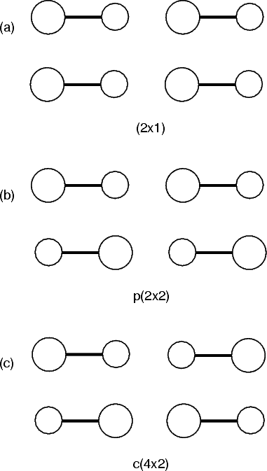
The silicon surface was first observed in 1959 in a LEED (Low Energy Electron Diffraction) study by Schlier and Farnsworth (1959). They found evidence for a (2x1) periodicity, which they attributed to a reconstruction based on dimer formation. Further investigations showed evidence of higher periodicities (p(2x2) and c(4x2) for example) which depended on sample preparation and treatment. A variety of models were proposed, which featured dimer models, and various other more drastic reconstructions (e.g. the dimer plus chain model of Northrup (1985) or the vacancy model of Poppendieck, Ngoc and Webb (1978)).
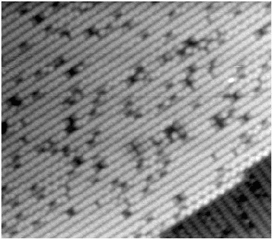
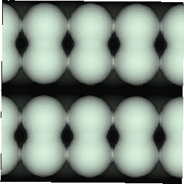
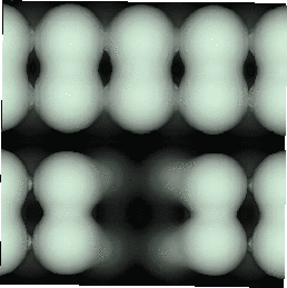
With the advent of STM, a real space image of the silicon surface could be obtained, an example of which is shown in Fig. 4.1. Tromp, Hamers and Demuth did just this (1985) and followed it up with a more comprehensive paper (Hamers, Tromp and Demuth 1986) in which they compared the various models to their pictures. This effectively established the dimer as the basic unit of the surface reconstruction1. However, further controversy ensued. There was significant doubt about whether the dimers were symmetric or buckled (as first suggested by Chadi (1979)), and also about the high level of defects in the surface. A schematic diagram of the different reconstructions is shown in figure 4.2.
|
Various different modellers predicted that symmetric (Pandey 1985, Ihara et al. 1990) or buckled (Chadi 1979,Roberts and Needs 1990) dimers were more stable - the essential point being that the energy difference between the two was small. Symmetric dimers seemed unlikely, as the surface would become metallic due to the degeneracy of surface states. The question as to why dimers might appear symmetric in the STM if they were really buckled was answered with the idea that they were flipping very quickly between the two possible buckled states (Dabrowski and Scheffler 1992). The breakthrough in understanding came when Wolkow (1992) imaged the Si(001)-(2x1) surface as he cooled it to 120 K. He saw a significant increase in the number of buckled dimers as he cooled, finding a maximum of 80% buckling at 120 K. He also observed (as have others) that buckling at room temperature occurs next to step edges and defects, where pinning will raise the barrier for flipping.
The conclusion which can be drawn from all of this work is that the silicon (001) surface consists of alternately buckled dimers which are bistable, and oscillate backwards and forwards between their two states. Previous calculations which found that the symmetric orientation was more stable may well have been insufficiently converged (Dabrowski and Scheffler 1992), and a recent study (Ramstad, Brocks and Kelly 1995) has found that, with insufficient convergence with respect to plane waves, symmetric dimers are more stable, and that the difference between p(2x2) and c(4x2) is too small to resolve accurately in LDA.
As a demonstration of the tight binding parameterisation which will be used throughout this work, I have performed calculations of the energetics of the three different reconstructions described above, using the standard unit cell. Relative to the c(4x2), which was found to be (just) the most stable, the p(2x2) has an excess surface energy of 0.1 meV per dimer (which is well below the limit of resolution of LDA, let alone tight binding; essentially the conclusion to draw here is that they are equally stable) and the (2x1) has an excess surface energy of 77 meV per dimer, which is in good agreement with LDA calculations. In general, I have used the p(2x2) reconstruction in this work, as the unit cells are a factor of two smaller, and, when working with steps, less complex.
It was recently observed (Owen et al. 1995) that, at low imaging voltages (i.e. relatively near to the Fermi level), the single missing dimer defect on the Si(001) surface appears to have been enhanced - the dimers either side of it brighten markedly. In this section, the behaviour is presented, and modelling solutions from both LDA and TB are given, along with a simple physical interpretation of the phenomenon.
In STM images of the Si(001) surface, for instance Fig. 4.1, there are always a certain number of dark features, which have been attributed variously to dimer vacancies (DVs) (Tromp, Hamers and Demuth 1985; Hamers, Tromp and Demuth 1986), adsorbed water molecules (Anderson and Köhler 1993) and interstitial dimers (Ihara et al. 1990). In the experiments which were performed (details of which are given in Owen et al. (1995)), there was almost no change in the appearance of the surface between room temperature and 400oC, by which time water should have desorbed. The interstitial dimer has been found to be unstable in the extensive modelling study of defects by Wang, Arias and Joannopoulos (1993), and so the majority of the dark features seen on the surface are taken to be missing dimer defects2, known as 1DVs (or, if two dimers are missing, 2DVs, etc).
These defects have a local effect upon the surface, which may be important in adsorption or desorption (Wu, Ionova and Carter 1993) or processes such as diffusion (Roland and Gilmer 1993). Recently, Carter and Carter have found evidence that the key factor in surface reactivity is the number of dangling bonds on the surface (Carter and Carter 1995) which will be affected by the structure of a defect. The structure of defects is therefore important when studying reactions on the surface.
When a single dimer is removed, the exposed second-layer atoms can either move apart and relax without forming bonds across the gap, or move together to form bonds across the gap, as had been first suggested by Pandey (1985). Wang, Arias and Joannopoulos (1993), in a careful study of defect structures and energetics using LDA, calculated the latter structure to be lower in energy by 0.42 eV. Since the two proposed structures have different numbers of dangling bonds, they might be expected to have different electronic structures and reactivities. Hamers and Köhler (1990) found using Scanning Tunneling Spectroscopy (STS) that the surface near 1-DV and 2-DV defects has a reduced band gap compared to the perfect surface. It was not known, however, which of the two proposed structures would lead to a reduced band gap.
|
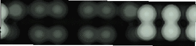
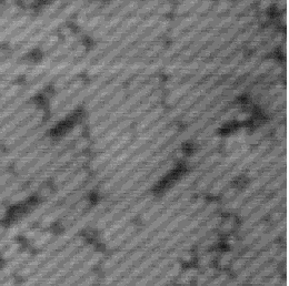
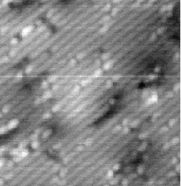
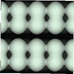
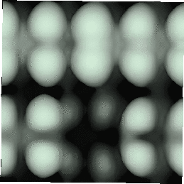
Images of the same area of the Si(001) surface at two different bias voltages (-1V and -0.6V) are shown in Figure 4.3(a) and (b). While the resolution is not good enough to make out individual dimers, defects can be seen as dark features of various sizes in the dimer rows. The image at lower bias voltage, i.e. nearer to the Fermi level (Fig. 4.3(b)), shows a marked change from the image at higher bias voltage ((Fig. 4.3(a)). The most common feature, the 1DV, is now highlighted on either side with a white patch. It is clear that this must be an electronic effect, as the only change between images is of bias voltage. This is indicative of a localised state further into the band gap than for normal dimers, which is the cause of the reduced band gap found by Hamers and Köhler. It is interesting to note that around some other defects, typically larger ones, a darkening is visible, which is indicative of a lack of charge or a surface state which is further out of the band gap than for normal dimers. For both of these features, it is the dimers either side of the defect which are affected, rather than the defect itself.
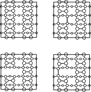
Three possible structures for the defect were modelled with TB (illustrated schematically in Figure 4.4): with the second layer atoms forming a bond across the gap (‘bonded’); with the second layer atoms relaxing away from the gap (‘broken’); and with one pair bonding across the gap and the other pair relaxing away from it (‘twisted’). A unit cell consisting of two standard unit cells side-by-side was used, making a cell six dimers long, and two dimer rows wide. A single defect was created in one of the rows. This found that the bonded defect was 0.45 eV lower in energy than the broken defect - a value remarkably close to that of Wang, Arias and Joannopoulos (1993). The twisted structure was the highest in energy.
|
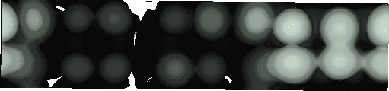
The charge density for the system was found by putting a reduced version of the tight binding unit cell into CASTEP , without re-relaxing the atomic coordinates. The dimer rows were truncated to four dimers in length, and the slab was reduced to 5 layers of silicon. The top 25 Kohn-Sham eigenstates were then projected out, with their energies given by the corresponding Kohn-Sham eigenvalues. STM images were simulated in a crude, but in this case effective, manner. The density of states in the tip was taken to be uniform, with the occupation given by a Fermi function with kT=0.025eV. The imaging bias was represented by an offset between the Fermi level in the tip and the sample. The contribution of each eigenstate in the sample to the tunneling current was taken to be equal to the available density of states in the tip. The tip was taken to be point-like, which results in a much improved resolution over the real STM images.
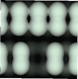
The results of this modelling for the bonded and broken structure are shown in Figure 4.5, along with the clean surface for comparison. At high bias voltage (left hand column), the two structures look extremely similar, with the dimers either side of the defect being virtually indistinguishable. At low bias voltage (right hand column), the situation has changed greatly. The bonded structure shows an enhancement of the dimers either side of the defect, whereas the broken structure shows a clear darkening of the dimers either side of the defect.
|
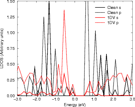
One interesting method of comparison between STM and theoretical calculations is via LDOS: the STM tunneling current (and hence the contrast seen) is in some way related to the LDOS for each atom. The result of a tight binding calculation in k-space (which used the same cell and parameters as before) giving the LDOS for the up atoms of a dimer on a perfect Si surface, and a dimer next to a rebonded 1DV are shown in Figure 4.6.
|
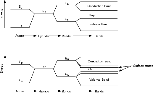
Fig. 4.6 clearly shows (for filled states only, as discussed in Chapter 3) that there is a change in the surface states in the band gap for the dimer next to the 1DV, yielding a large state close to the Fermi level. This state is what is responsible for the enhancement. A simple LCAO argument demonstrating how this works is given in Figure 4.7. As the electronic states progress from atomic orbital levels to hydrids and then bonds and bands, the structure becomes more complex. At the top of Fig. 4.7, the situation is shown for bulk Si, which forms perfect tetrahedral bonds at 109.3o. This bonding and structure give rise to the band gap which makes Si an insulator. Below this is a picture of what happens at the surface. The atoms in the dimers are pulled away from the perfect tetrahedral angle, which reduces the bonding-antibonding splitting at the bond stage, and results in bands in the gap - also known as surface states. The picture would change even further if more constraint were put on the dimers - for instance by second layer bonding which pulls them away from the equilibrium dimer position. This is clearly what is happening in the STM images shown in Fig. 4.3(b), resulting in the enhanced behaviour either side of the defect. As an extension to this, consider what would happen if the second layer atoms were allowed to relax. In this case, the dimers would be closer to their equilibrium structures (i.e. the bulk structure) and the surface states pushed away from the Fermi level. This explains the darkened appearance of the broken defect, and suggests that any darker areas on the surface (as seen in Fig. 4.3(b)) are associated with relaxed bonds and structures similar to the broken defect.
|
Thus the structure of the 1DV has been identified conclusively, and it is actually less reactive than the normal surface, as one dimer is missing and the second layer is rebonded. Defects need not enter into calculations of reactions, unless specifically desired.
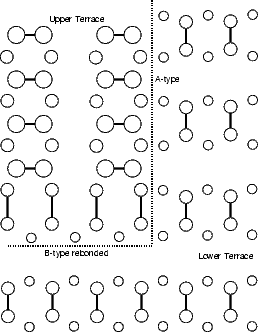
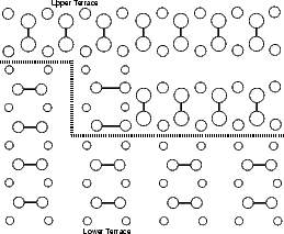
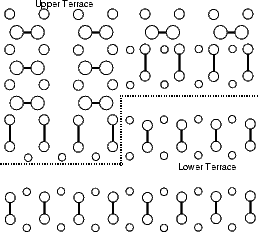
Si(001) wafers, as obtained by cleaving from a boule grown commercially, are not perfectly flat. Indeed, there will be a large step density on the surface, though this can vary from area to area. There are two kinds of steps, because of the (2x1) periodicity: one where the dimer rows in the upper terrace are parallel to the step edge (A-type) and the other where they are perpendicular to the step edge (B-type); these are illustrated in Figure 4.8. The B-type step edge has two possible terminations (the unbonded and the rebonded) depending on where the step ends relative to the dimer rows in the lower terrace - the rebonded is shown in Fig. 4.8, and the unbonded would have another dimer in the upper terrace, removing the lower terrace dimers just above the dotted line.
|
The A-type step is generally very long and straight, with an occasional kink seen at room temperature, whereas the B-type step is seen to be kinked often at room temperature. In this section, we shall examine the size of unit cell required to model steps successfully, and the kinking energy for A-type and rebonded B-type steps.
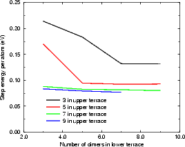
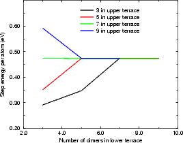
In the repeated supercell method of simulation (as described in Chapter 2), care must be taken to isolate features in one cell from their images in other cells. This is generally done by making the cell large enough that any interaction is negligible. With steps, the isolation must be achieved across two terraces, one at a lower level and one at an upper level. The excess surface energy for rebonded and unbonded B-type steps and for the A-type step have been calculated using tight binding. The standard unit cell was used, but lengthened (to lengths given in the figures, up to 18 dimers long) and with some of the top layer removed to give a pair of steps. These are shown in Figures 4.9 and 4.10.
|
To calculate the excess step energy for these cells, I found the excess surface energy (i.e. Ecell -n×Ebulk, where there are n atoms in the unit cell and the energy for a bulk silicon atom is Ebulk) for the stepped cell and a clean, unstepped surface of the same surface area. The excess step energy is then given by the difference between these two (though divided by two, as there are two steps in the unit cell). There was no need to compensate for the hydrogen termination in these calculations as the termination energy was the same for each cell, and cancelled.
The calculation was not quite that simple, however. The lower terrace has only four layers of silicon atoms before the bulk-like silicon, whereas the upper terrace has five layers. The difference in excess surface energy between the four layer and five layer cases is only 0.02 eV per dimer, but without this correction the step energy shown in the figures has a linear increase, which would lead to an infinite energy at infinite separation.
The final values show that for the B-type step, the energy is converged with respect to the lower terrace within 5 dimers, and with respect to the upper terrace within 5 or 7 dimers. The values per atom shown in Figure 4.9 (a) and (b) are 0.08 eV/a for the rebonded step and 0.473 eV/a for the unbonded step. The A-type step is less sensitive to cell size, and is converged for all values of upper terrace width, and beyond four dimers in the lower terrace. The value of energy per surface lattice constant is 0.019 eV. It should be noted that the scale in Figure 4.10 is ten times finer that in Figure 4.9(b) leading to the appearance of poorer convergence.
There are several values to compare these energies against. Chadi (1987) calculated the structures and energies
of single and double height steps on the Si(001) surface using tight binding. He found a value of 0.01
eV/atom for the A type step, 0.075 eV/atom for the rebonded B type step and that the unbonded step is
“energetically less favourable by at least 0.16 eV/atom”. The only other quantum mechanical study (Bogus awski et al. 1994) used DFT, but only had 3 dimers in the upper terrace and did not quote step edge
energies, so is not very helpful. The experimental evidence will be discussed fully in the section on
kinks.
awski et al. 1994) used DFT, but only had 3 dimers in the upper terrace and did not quote step edge
energies, so is not very helpful. The experimental evidence will be discussed fully in the section on
kinks.
In the same way that certain defects show an enhancement at low imaging voltage, so also certain step edges show this enhancement. An example of this is shown in Figure 4.11.
|
The significance of this enhancement extends to two other chapters; both the stability and diffusion of hydrogen near step edges depends on the structure of the step in question (Chapter 6) and the growth of silicon occurs at step edges and islands, but may be inhibited by hydrogen (Chapter 7). The rebonded B-type step (which is the lower energy termination) bears a great deal of similarity to one half of the rebonded defect discussed earlier, and might be expected to have the same enhancement behaviour seen before for that system. Accordingly, a similar calculation was performed for the unbonded and rebonded B-type steps as was performed for the defect, using LDA.
|
|
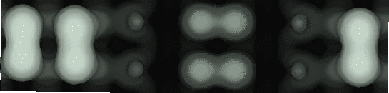
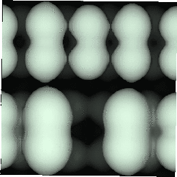
The unit cell used was eight dimers long, and five layers deep, with the bottom layer constrained to lie in bulk-like positions, and terminated with hydrogen. Five of the top layer dimers were removed, to create a double step in the unit cell, which was only three dimers long. While this may seem contradictory to the conclusions drawn above about length of step required, the cell was only being used for charge densities and not energetics, and the positions, and hence strains, for the atoms are acceptably similar to a larger cell. This choice was a compromise between isolation and computational possibility, as a larger cell would have been prohibitively slow. To obtain symmetrical images, as would be seen in STM, two calculations had to be performed with the dimers in the second calculation flipped the other way to the dimers in the first calculation. The charge densities were then added to show a symmetrical image. The simulated STM images for the rebonded step edge are shown in Fig. 4.12, and for the unbonded step edge in Fig. 4.13. Clearly, the same effect is at work here as in the defect case, and an enhanced step edge can be taken to be a B-type rebonded step edge (the A-type or B-type identification is made from the direction of the dimers in the upper terrace).
|
|
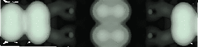
There is a question about the saturation of step edges with hydrogen during disilane growth which will be addressed fully in Chapters 6 and 7. The essence of the question is whether or not saturating the bottom of the step will promote or decrease the enhancement at the top. This can be easily answered by using the same technique as above, and the simulated images are shown in Figure 4.14.
|
|
It is clear that the hydrogenation of the bottom part of the step does not stop the enhancement of the step, and that this should not be taken as a counter to the argument in Chapters 6 and 7.
At growth temperatures, the step edges on the Si(001) surface become mobile, and kinks are seen to form and move around. Kinks3 in the A-type and B-type steps are illustrated schematically in Figure 4.15. At room temperature, the A-type step is extremely smooth, while the B-type step kinks frequently, and appears rough. The step edges can play a large part in the surface dynamics of growth, and understanding the energetics of kinking is important. There has been a large amount of experimental work on step kinking (Pearson et al. 1995a; Pearson et al. 1995b; Swartzentruber et al. 1990; Swartzentruber et al. 1993; Bartelt, Tromp and Williams 1994; Zandvliet et al. 1992) which has produced various results: firstly, the step edges energies mentioned above, along with a “corner” energy (that is, the energy generated by the corners of a kink); secondly, the energetic behaviour of the separation and depth of kinks; finally, the dynamics of kink formation, diffusion and extinction. As the majority of results are for the B-type step kinks, these will be presented first.
|
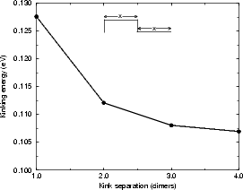
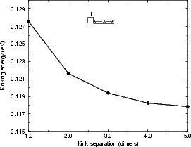
As was the case with the step energies discussed above, it is important to understand how big the supercell must be to prevent kinks from interacting. Two cells were investigated using TB, both of which had two kinks (one up and one down) of depth two atoms (this terminology may be confusing; the kink depth is exactly as illustrated in Fig. 4.15 for the B-type step, where the depth is two atoms). The unit cell was the equivalent of 14 dimers long, with four dimer rows, and the usual depth and termination. In the first cell, the separation of the kinks in both directions was increased simultaneously, whereas in the second, only one segment of step edge was lengthened. These cells are illustrated schematically in the insets of Figure 4.16 and the energies for the kinks are given for the first case in Fig. 4.16(a), and in the second case in Fig. 4.16(b). From these it can be seen that the energy associated with a kink is converging to a limit with separation, and that the kink-kink interaction is small even with two dimer rows separation (less than 0.01 eV) and negligible at three. The kinking energy of the B-type step for a cell with a kink of depth one atom was also investigated, and proved to be 1.04 eV - mainly because of the unfavourable unbonded termination forced by the depth of one dimer. Kinks of depth one are almost never seen in experiment, and therefore will be discounted.
|
Now that the isolation issue has been addressed, the first question to be answered is that of how best to compare
with experimental results. All subsequent experimental papers rely on the analysis of Swartzentruber et al. (1990),
whose formalism will be examined in detail, and a useful extension derived. To summarise their assertions, they said
that when examining the kinks on a B-type step, there are two distributions: firstly, the separation of kinks, s,
which behaves as P(s) = Pk(1 -Pk)s/2-1, where Pk is the probability of any kink at the site under consideration;
secondly the depth of a given kink, n, which has a probability proportional to the expontential of its energy,
P(n)  exp
exp![[(-neA + EC)/kT ]](Master142x.gif) , where
, where  A is the energy of the step exposed when kinking (the A-type
step).
A is the energy of the step exposed when kinking (the A-type
step).
To understand these better, consider an arbitrary length of B-type step with a step energy of B. If we introduce
a kink into this system, the energy will be raised by nA + EC, where n is the depth of the kink, A is the energy of
the step edge exposed and EC is the “corner energy”. The probability of this kink occuring will be, as
stated above, proportional to the exponential of its energy. The probability of any kink occurring at a
given site is then simply the sum over the probabilities of all kinks, divided by the partition function:
![P(n) = exp[- (neA + EC) /kT]/Z, (4.1)
oo sum
Z = 1+ 2 exp[- (neA + EC)/kT ], (4.2)
n=1
sum o o
Pk = 2--n=1-P(n),
Z
= ---------2exp[(--eA--EC)-/kT]---------, (4.3)
1 -exp (- eA/kT) + 2exp [(-eA - EC) /kT]](Master143x.gif) A and EC from plots of P(n). Thus the values available for comparison with experiment
are P(s), A and EC. All of these absolute quantities depend on the temperature at which the step edge is
assumed to have equilibrated, which is not known; the ratio A/EC is a more independent measure of
the accuracy of the calculation, and can be used for comparisons with the theoretical results. It is
possible to obtain a good estimate of the temperature by comparison with the theoretical results, once
validated.
A and EC from plots of P(n). Thus the values available for comparison with experiment
are P(s), A and EC. All of these absolute quantities depend on the temperature at which the step edge is
assumed to have equilibrated, which is not known; the ratio A/EC is a more independent measure of
the accuracy of the calculation, and can be used for comparisons with the theoretical results. It is
possible to obtain a good estimate of the temperature by comparison with the theoretical results, once
validated.
|
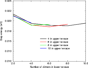
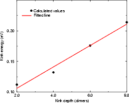
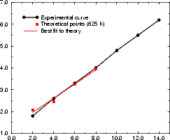
Figure 4.17(a) shows the variation of kink energy with a depth ranging from 2 to 8 atoms for a rebonded B-type step, calculated using TB. The unit cells used ensured that there was always a separation of five dimers between steps adjacent to kinks, so that the length varied between 14 and 26 dimers. The configuration is as shown in Fig. 4.15 for a depth of two atoms, and consists of two dimer rows, a kink up, two dimer rows and a kink down, repeating infinitely. The separation between kinks of two dimer rows was chosen as a compromise between accuracy and feasibility - the kink of depth eight dimers had 2,500 atoms in the unit cell. The line shown is a best fit, and gives a step edge energy for the A-type step exposed of 0.018 eV (which should be compared to 0.019 found in Section 4.3.1 and differs by only 1 meV) and a corner energy of 0.071 eV. These have a ratio of 0.246. Fig. 4.17(b) shows the experimental line for E(n)/kT from Swartzentruber et al. (1990), along with the same theoretical points in (a), but scaled with a kT appropriate for 625 K. The close correspondence suggests that the appropriate temperature to use for these experimental results is 625 K. The issue of temperature is discussed more fully below.
All the experimental papers to be described measured the kink distributions with an STM at room temperature
(except where stated). The sample was annealed at a high temperature, and radiation quenched to room
temperature to perform observations. This procedure leads to a large uncertainty in the temperature used to obtain
absolute values for energies. Swartzentruber et al. (1990) found values of A/kT=0.37±0.03 eV and
EC/kT=1.1±0.3 eV; the errors on A/kT and EC/kT are correlated, so that if A/kT goes up, EC/kT goes down
(this arises from fitting a straight line to the experimental data). The ratio for the values given is
0.336, but going one standard deviation away to 0.34 and 1.4 gives 0.243 - so the values are well within
experimental error of the theoretical results. A temperature of 875K was assumed, which gives absolute
values of A=0.028 eV and EC=0.09 eV; in a later paper (Swartzentruber et al. 1993), a value of 625K
is quoted, which gives values of A=0.02±0.01 eV and EC=0.06±0.01 eV, which is in much better
agreement. Given later studies (Swartzentruber and Schacht 1995; Kitamura et al. 1993; Zandvliet,
Elswijk and van Loenen 1992; Pearson et al. 1995a,b) which suggest that step edges start to move
on a timescale of tens of seconds at between 550 and 600 K, this value of 625K seems much more
reasonable, and fits well with the value derived from theoretical results. A temperature which agrees with
A, EC and Pk will be given below. Other measurements of step kink distributions give results of:
A=0.026 eV and EC=0.06 eV, with a ratio of 0.43 (Zandvliet et al. 1992), though these results include
kinks forced by the miscut of the crystal which will give a low value of EC and a correspondingly
high value of the ratio; and A=0.02 eV and EC=0.07 eV, with a value of B of 0.075 eV (Bartelt,
Tromp and Williams 1994). This last study used a relatively new technique known as LEEM (low
energy electron microscopy) which is a large area technique, resulting in relatively large errors in the
values found. Overall, the experimental results are in good agreement with the theoretical values found,
though the errors are sufficiently large that the best conclusion that can be drawn is that there is no
contradiction.
|
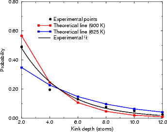
The final test of the results is to calculate a value of Pk from the theoretical values, using an appropriate value
of kT. This is shown in Figure 4.18 for kT equivalent to 625 K and 900 K, along with the experimental results from
Swartzentruber et al. (1990). The value of Pk is clearly highly dependent on the value of kT used, and the exact
ratio of A to EC; however, the theoretical curve for 625 K is a good fit except for the first point. The experimental
data as given in Swartzentruber et al. (1990) have no error bars, and cannot be made to fit the form of P(s)
for any value of Pk. A temperature of 625 K gives values of A and EC of 0.018 eV and 0.076 eV
for the set of experimental numbers which match the theoretical ratio; this, along with the good fit
obtained in Fig. 4.17(b), may be an indication of the effective temperature at which the steps were
quenched.
The kinking of an A-type step is rarer, but values of B have been found nevertheless, though assuming that the
corner energy is not different to that for a B-type step. To test this, a single calculation for the kinking of an A-type
step was performed with TB, using a standard unit cell which was ten dimers long, and five dimer rows
wide. This yielded a value for the corner energy of 0.078 eV, which is in almost exact agreement with
the value from B-type steps. This is reassuring, given that the corners are almost exactly identical,
and means that the energy found for the B-type step edge energy can be trusted. Swartzentruber
et al. (1990) found that B/kT = 1.2±0.1, but rather than using the E(n) plot above, they used a
probability. This gives a ratio of 1.09 or 0.86 for EC=1.1 or 1.4, and a value for B of 0.065±0.005
eV, which is a little lower than the value of 0.08 eV found in Section 4.3. As they give almost no
details of the calculation, it is hard to know where the differences might occur. The value obtained by
Bartelt, Tromp and Williams (1994) of 0.075 eV is in much better agreement with the calculated
results.
Conclusions In this chapter, the Si(001) surface has been introduced. After examining the reconstructions which characterise it, the effects of strain on bonding have been investigated, enabling the identification of a defect structure, and the confirmation of step structures. The structures and energetics of kinked steps have been studied, yielding good agreement with experiment. Now that the surface on its own has been examined, adsorbates can be added with confidence.