| Research |
| Teaching |
| Publications |
| DensEl |
| ParaDens |
| Conquest |
| Links |
| Home |
The Si(001) surface is characterised by rows of dimers (pairs of atoms bonded to each other, with each left with one dangling bond) - more details can be found here. If the surface is exposed to atomic hydrogen (not molecular hydrogen, which has a low sticking coefficient) each dangling bond becomes passivated with a hydrogen, and the surface becomes relatively inert. However, in the last few years, people have used scanned probe microscopes (such as the STM) to selectively remove hydrogens from the surface, leaving rows of exposed dangling bonds, which are being called "dangling bond wires":
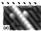
In the above image, the dimer rows are marked with arrows, and the dangling bond wire is imaged as a line of white protrusions from the surface (though only the "up" atoms are imaged).
Why are we interested in these wires ? They certainly wouldn't have much use as wires in any commercial devices, as they require a surface to exist, and only exist in ultra-high vacuum (UHV) conditions. Conduction in one dimension has a whole host of interesting properties which differ from normal 2D or 3D conduction, and this is a simple example system. We are specifically interested in the links between lattice distortions and charge carriers (polarons) and ordering defects (solitons).
Working with Andrew Fisher and two students (Milica Todorovic and Charlie Bird), I have been exploring the electronic and structural properties of this system:
Electronic structure of finite dangling bond wires
We have found that spin-polarisation is extremely important when performing first principles calculations of odd-length finite dangling bond wires. The height of the physical distortion of the wires is about a factor of five smaller (and in much better agreement with STM measurements) when spin polarisation is accounted for in calculations of the electronic and atomic structure of these wires. The spin difference density is shown below for a length five wire (click for more detail). Published as Surface Science 531-2, L531 (2003). (Work by Charles Bird)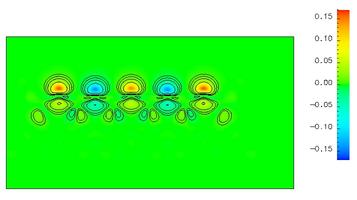
Polarons in dangling bond wires
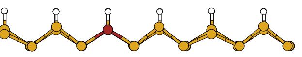
Using tight binding, we injected charges (both electron and hole) into a dangling bond wire, and found that they form polarons: a localisation of the charge associated with a distortion of the lattice. The hole polaron localises on an up atom, while the electron polaron localises on a down atom. Both these cases are illustrated below, where the dangling bond wire is seen in side view, and the location of the polaron is indicated by a dark-coloured atom. Published as Physical Review B 63 (3), 035310 (2001).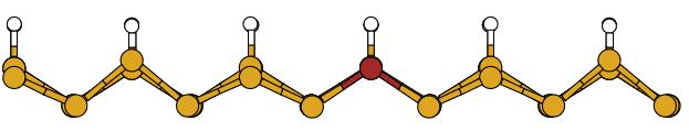
Mobility of polarons
As an extension of the above study, we have investigated the diffusion barrier to hopping of the polaron. Simple reaction dynamics failed, giving us only an upper bound on the barrier (0.12 eV), but elevated temperature molecular dynamics (along with analysis of the location of the top-most filled band) gave excellent results. Using an Arrhenius form for the hopping probability we found a diffusion barrier of 0.08eV. This work has been published as J. Phys.:Condens. Matter. 14, L749 (2002).(Work by Milica Todorovic as fourth year project).Solitons in dangling bond wires
By analogy with conducting polymers, as well as polarons, we could expect to find solitons (ordering defects) in dangling bond wires. The structure of the dangling bond wire is Peierls distorted (rather than an even line of exposed atoms, each with a half-filled bond, there is an alternating pattern of upward and downward displaced atoms, with charge transferring from the down to the up, not unlike the buckled dimer pattern seen on the clean Si(001) surface). A soliton is formed by two adjacent up or down atoms in the wire. We have investigated the atomic and electronic structure of these defects in finite wires, of both even and odd length, using tight binding. Published as Physical Review B 68, 115318 (2003). (Work by Charlie Bird.)