Research Images
 Self-assembley of hexagonal Bi2Te3 nanosheets on mica imaged by high-speed AFM
_cut.jpg) AFM of single layer TiS2 nanoshseets on mica
AFM of single layer TiS2 nanoshseets on mica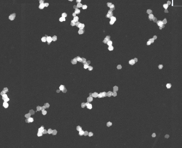 Scanning transmission electron microscopy of self assembled Bi2Te3 nanosheets deposited from solution
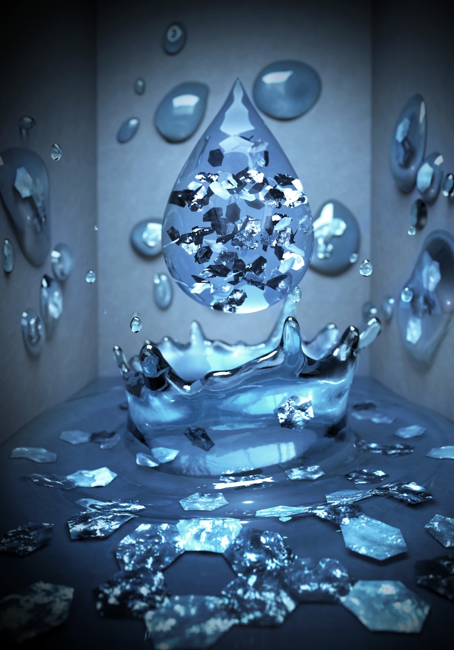 Artist impression of a nanosheet solution
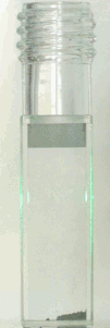 Potassium-intercalated Bi2Te3 spotaneously dissolving in DMF over 2 weeks
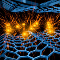 Artist impression of superconducting graphene sheets (credit SLAC)
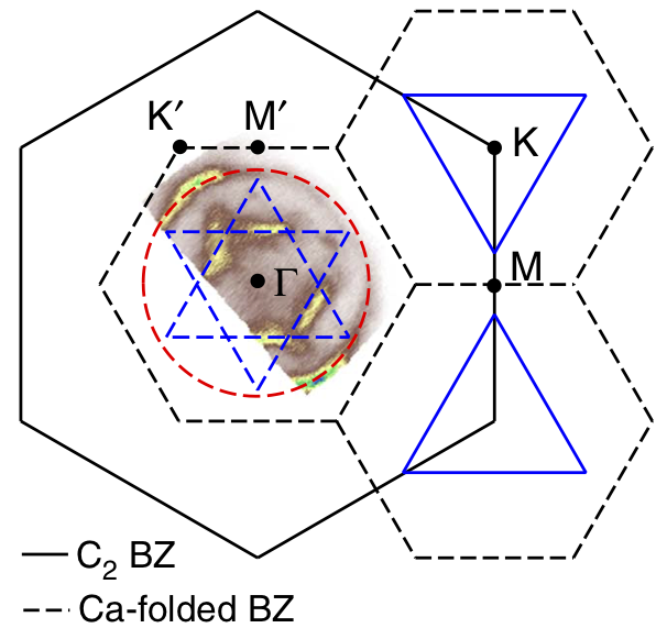 The band structure of heavily electron doped grpahite revealed by ARPES, showing the 2D graphitic pi* band and the 3D intercalant-derived IL band
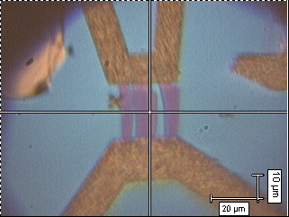 Optical micrograph of Mg doped bilayer graphene
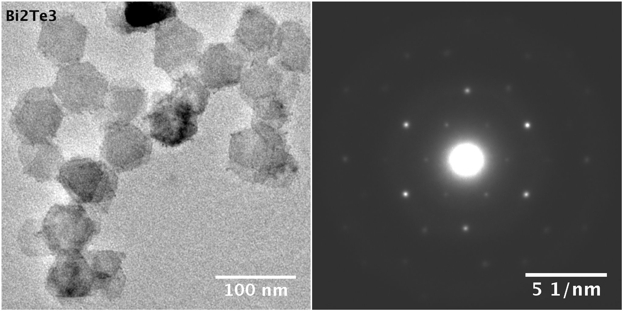 TEM (left) and electron diffraction (right) of single crystal, hexagonal Bi2Te3 nanohsheets deposited from solution
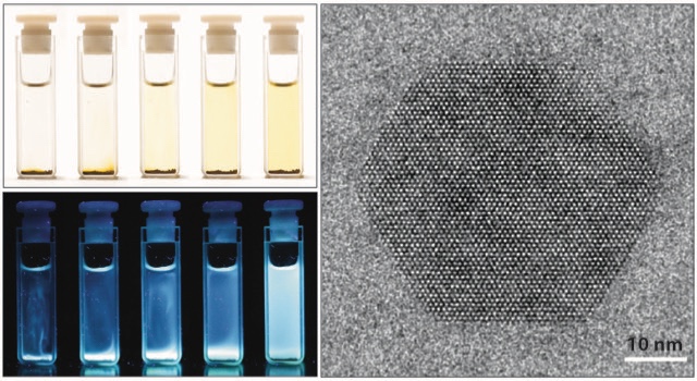 Spotaneous dissolution taken over 2 days (left) of luminescent, hexagonal carbon nitride nanosheets (right)
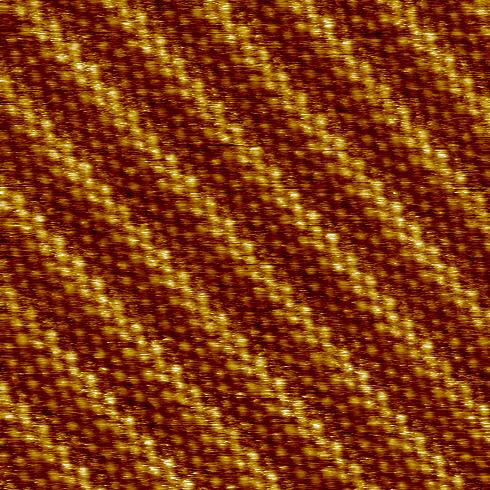 Raw STM data of the charge density wave on the graphene sheets of CaC6
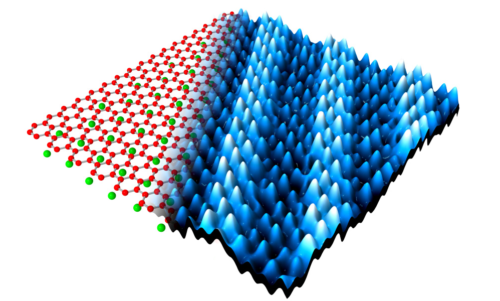 Charge density waves in CaC6
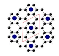 2 x 2 potassium superlattcie on graphene
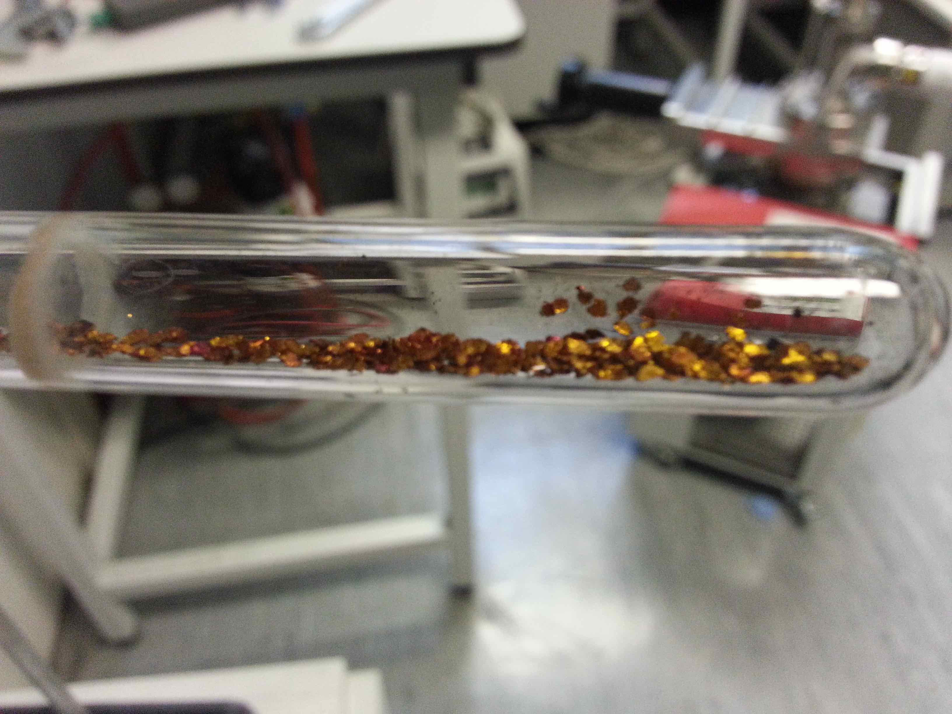 Stage 1 potassium intercalated graphite (madagascan flake graphite), KC8
 Potassium intercalated graphite (graphoil), KC8
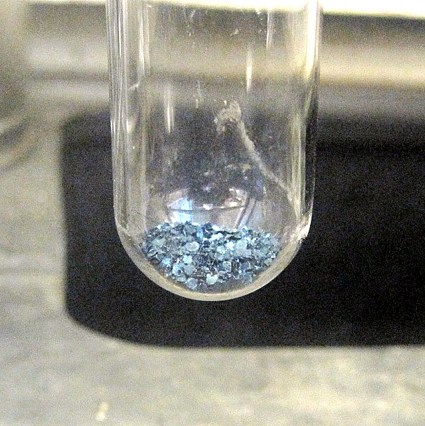 Intercalated graphite KC24(NH3)
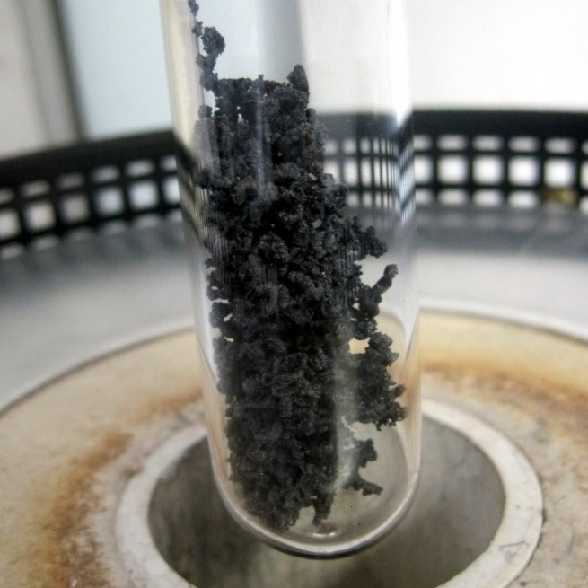 High surface area large, crystallite size exfoliated graphite
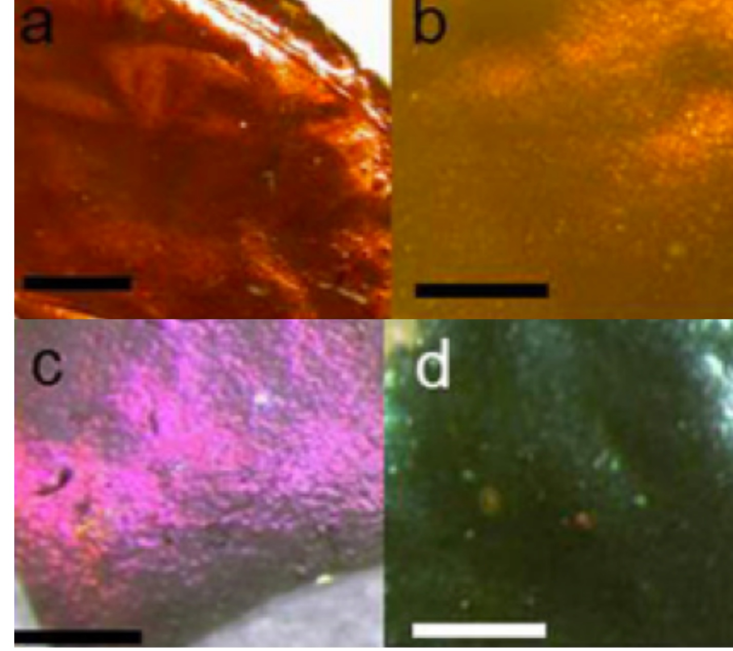 Calcium doped graphene (top left) and graphene hBN laminates
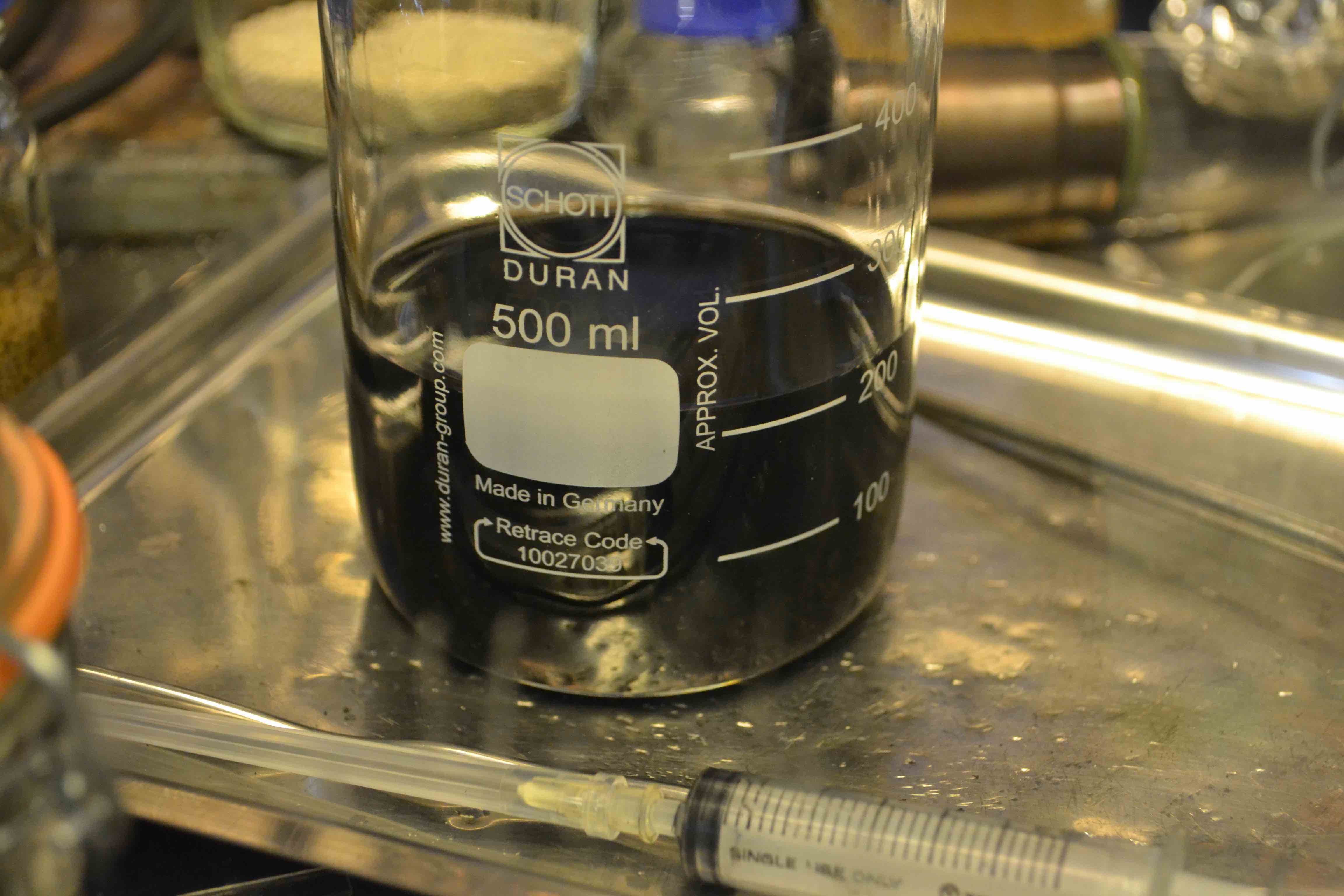 Solution of carbon nanotube anions in NMP
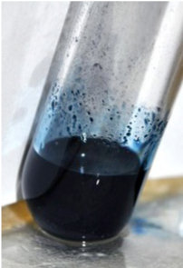 Li dissolved in liquid ammonia
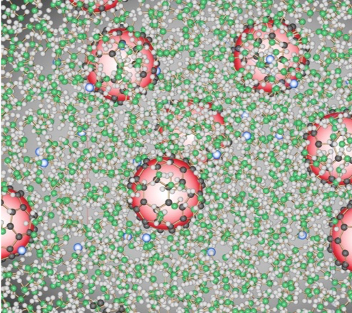 C60 anions in ammonia from neutron diffraction
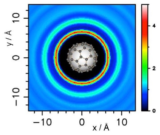 2D ammonia solvent probability density around dissolved C60 anions from neutron diffraction
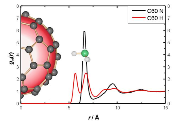 1D probability distribution functions of ammonia around C60 anions from neutron diffraction
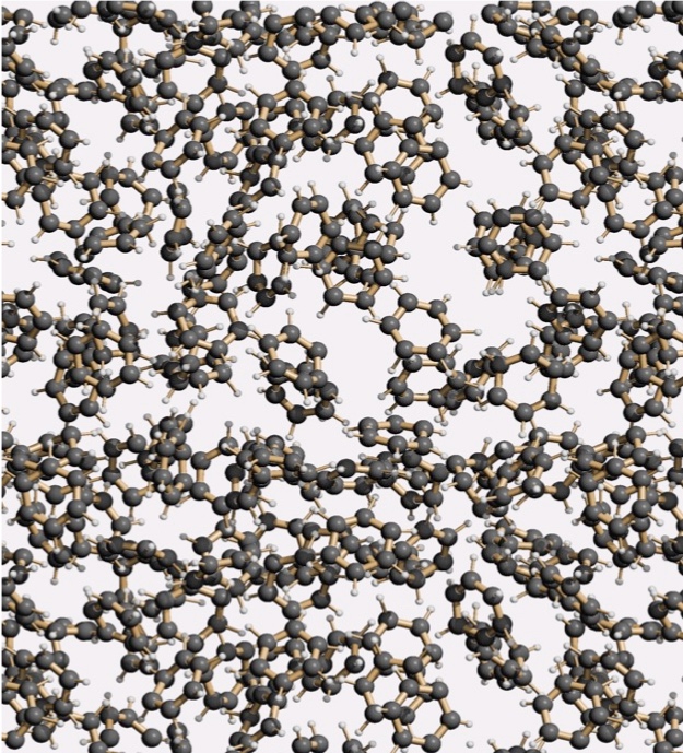 Structure of benzene from neutron diffraction
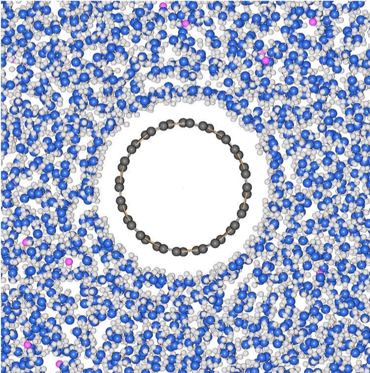 Monte carlo simulation of SWNT anions dissolved in liquid ammonia
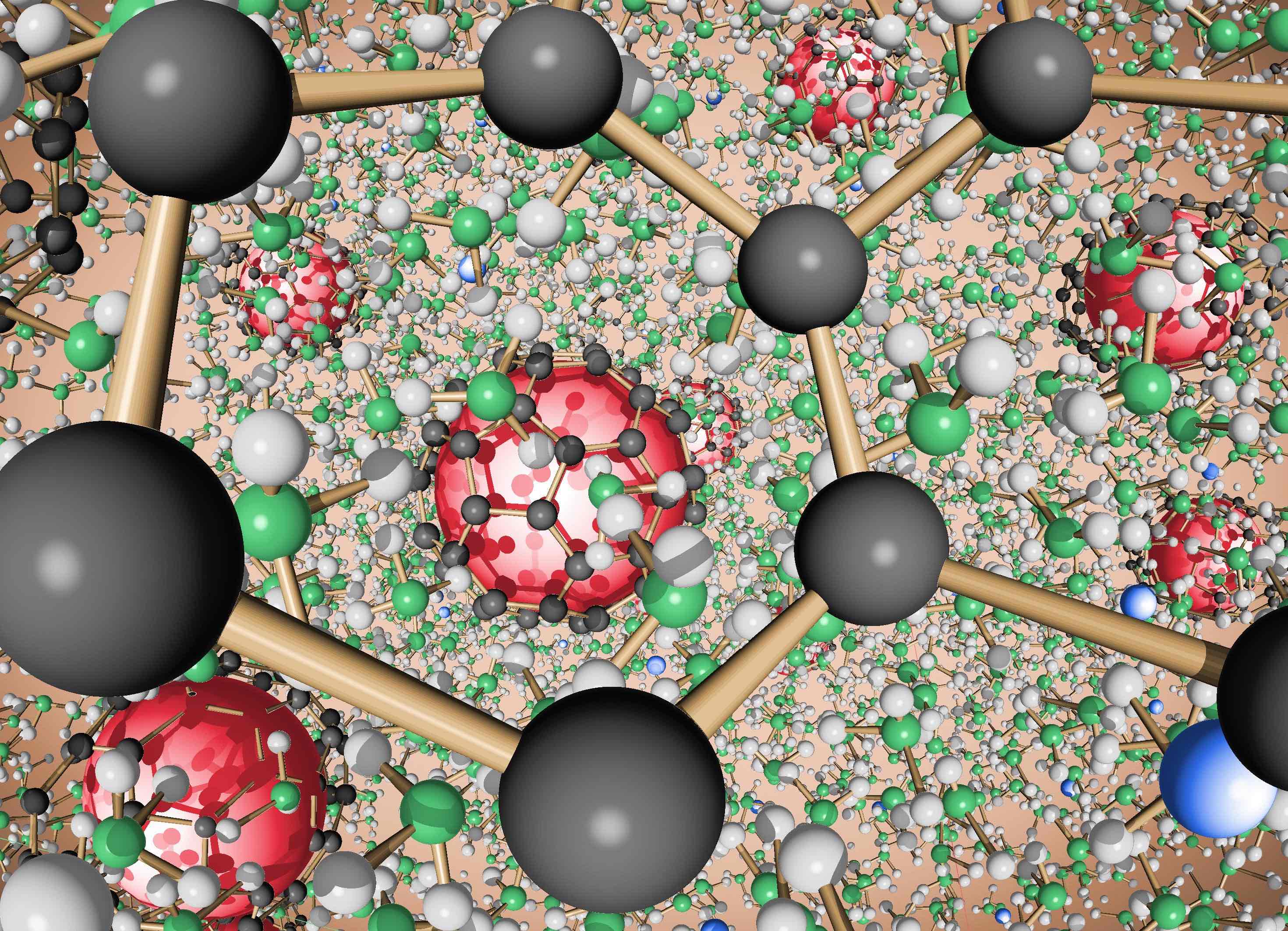 C60 anions in ammonia from modelled diffraction data
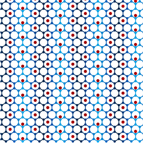 Schematic of the CDW on Ca-doped graphite
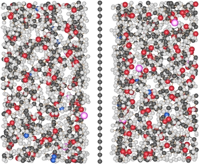 Monte Carlo simulation THF molecules around dissolved graphene sheets
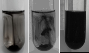 Na-Single Walled Carbon Nanotubes dissolving in DMF
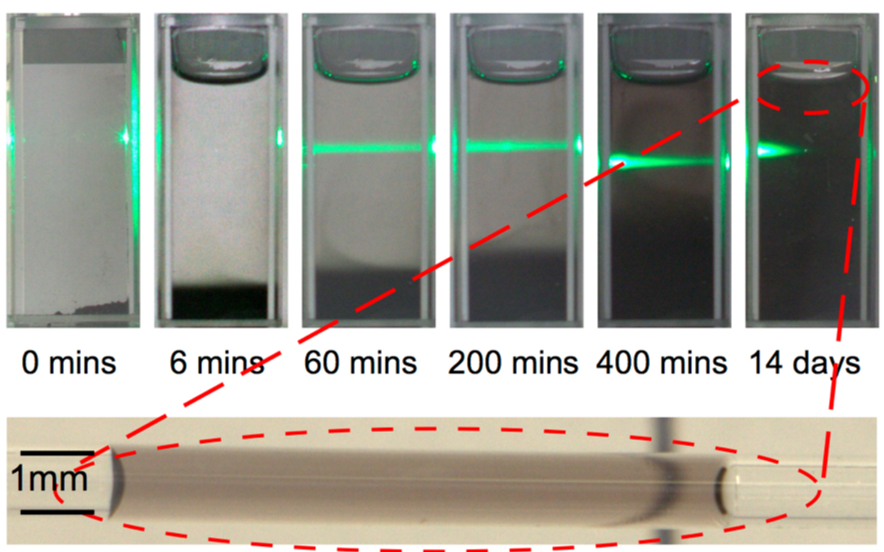 K-Bi2Te3dissolving
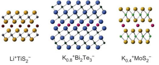 Intercalated materials we make
Phosphorene Nanoribbons
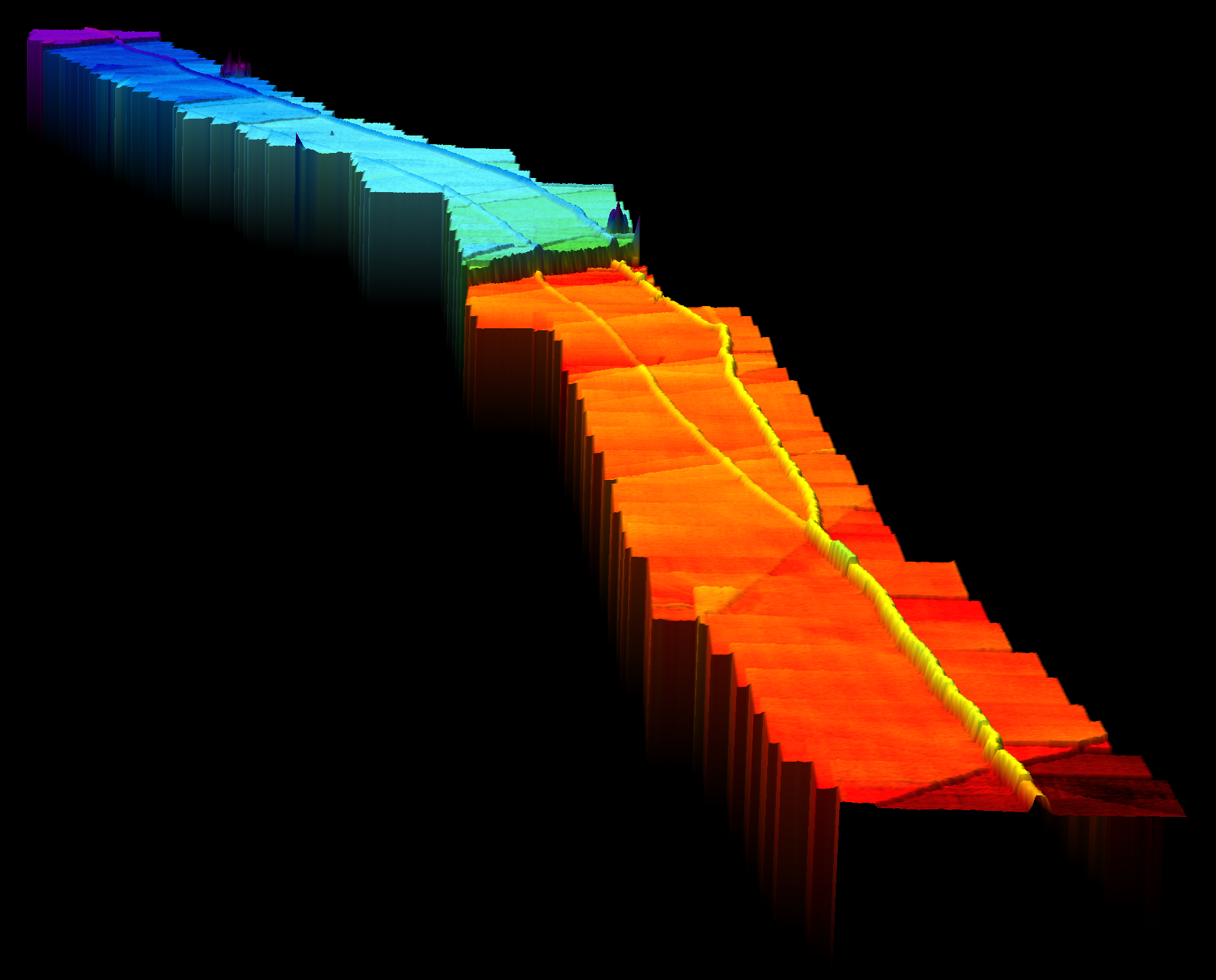 Stitched HS-AFM image of phosopherene nanoribbon (yellow) on a graphite substrate
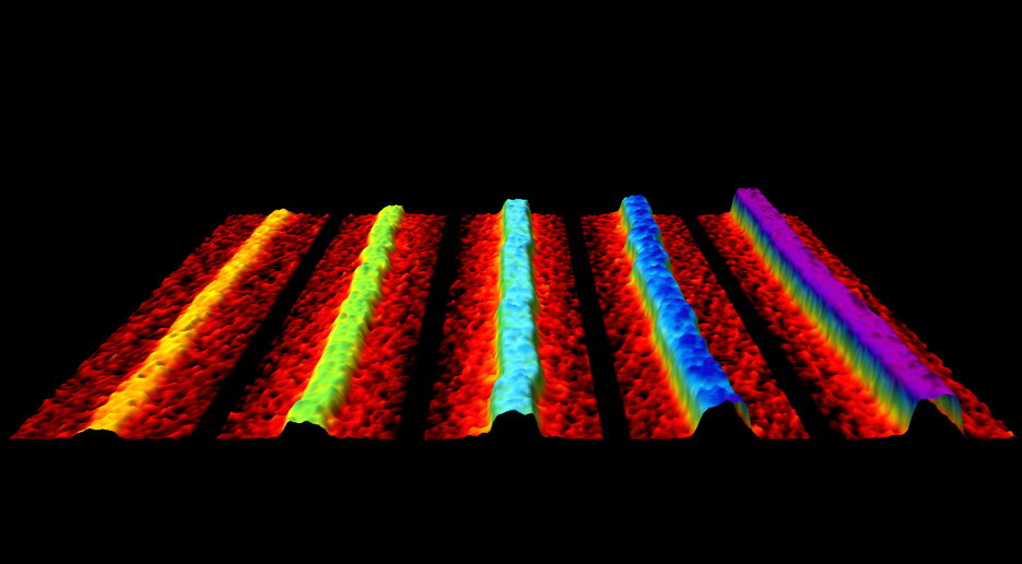 AFM micrographs of 1-5 layer high phosphorene nanoribbons
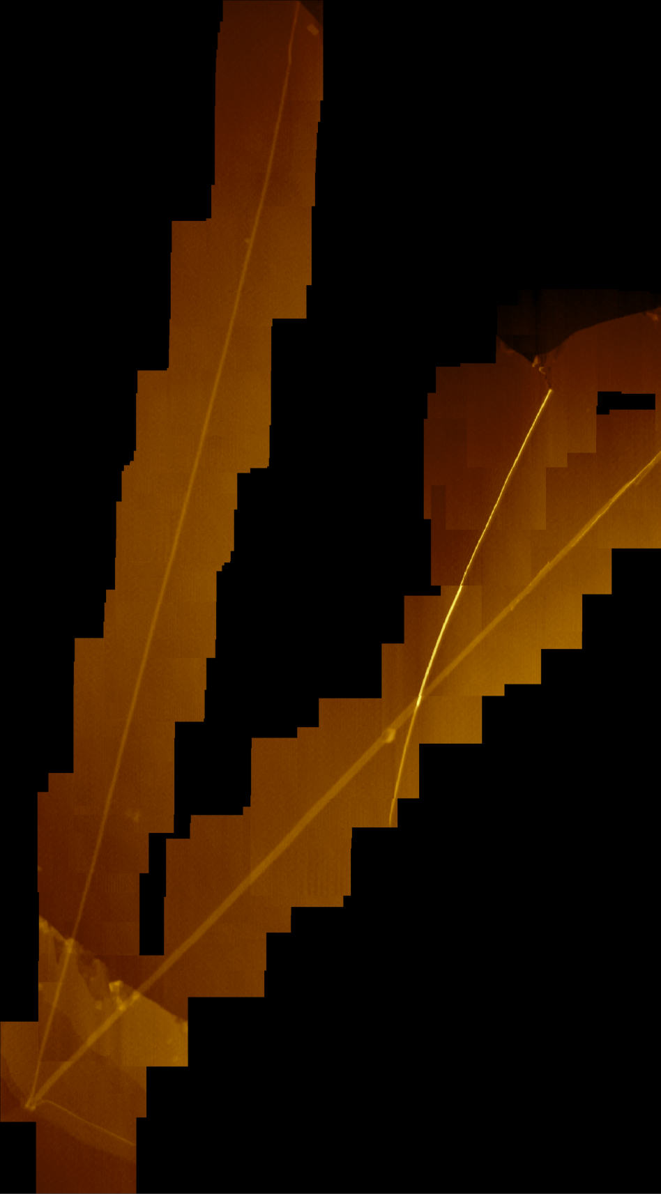 AFM of PNRs
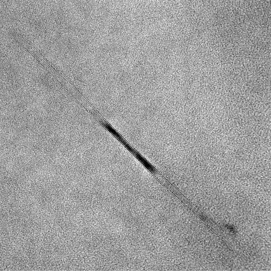 TEM of 3 nm wide PNR
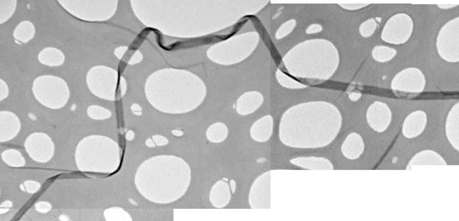 TEM of PNR draped on a holey carbon support
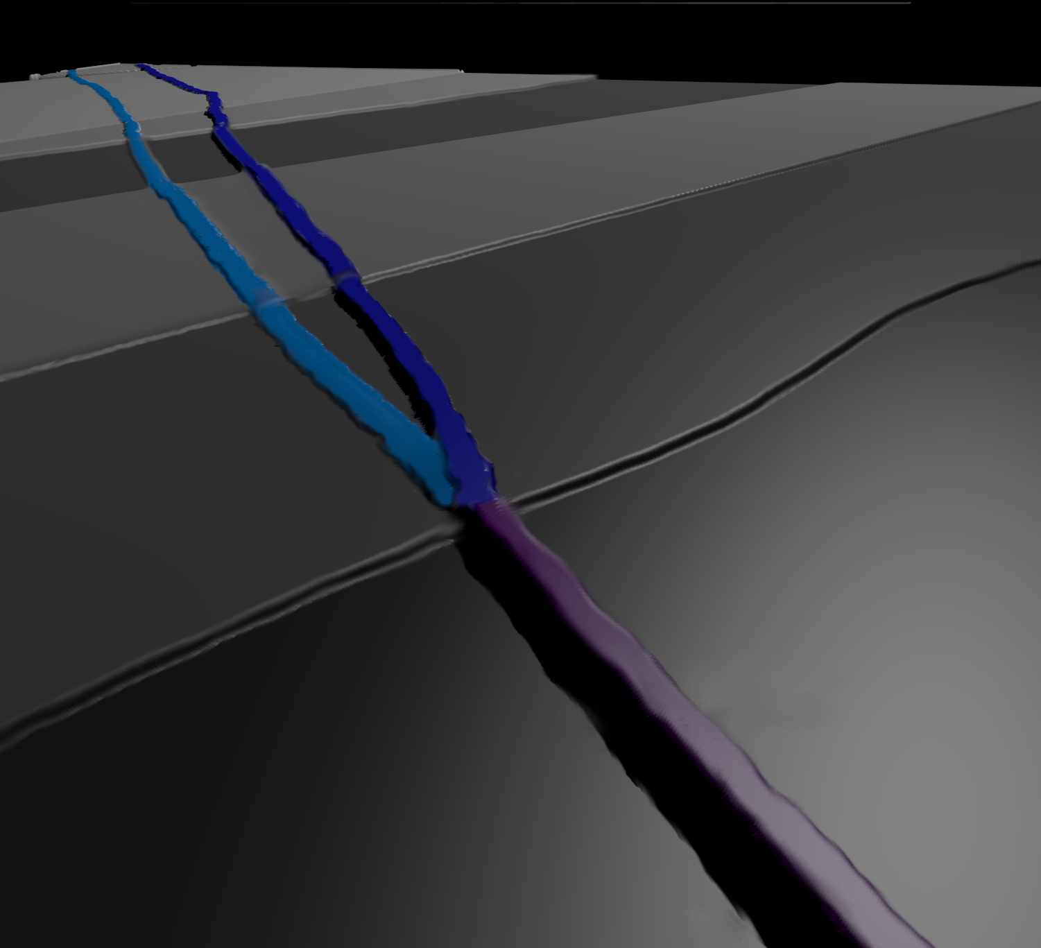 AFM of a 7 layer PNR (on a graphite surface) seamlessly spliting into a 2 and 5 layer
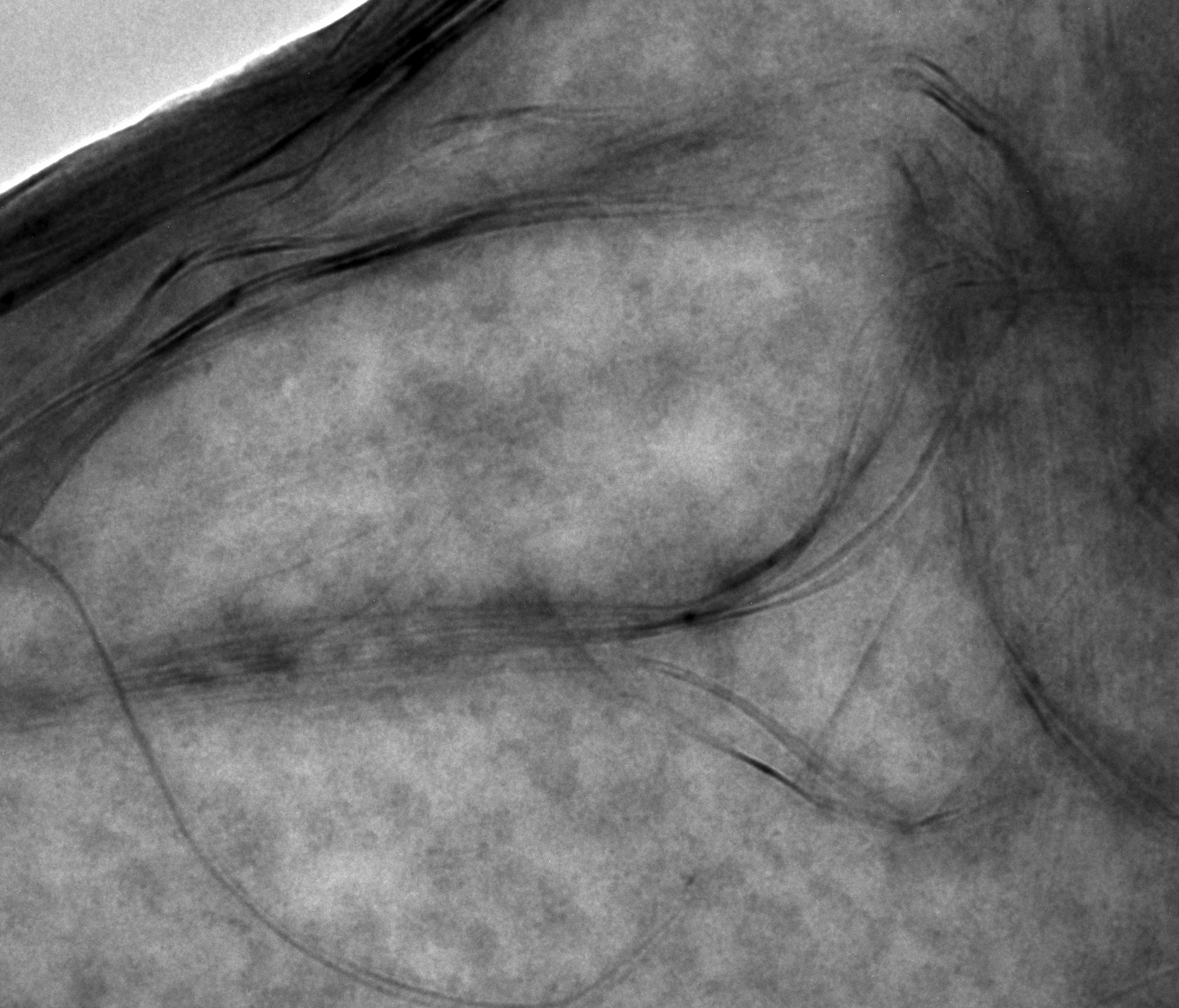 TEM of PNRs forming from a larger 2D phosphorene sheet
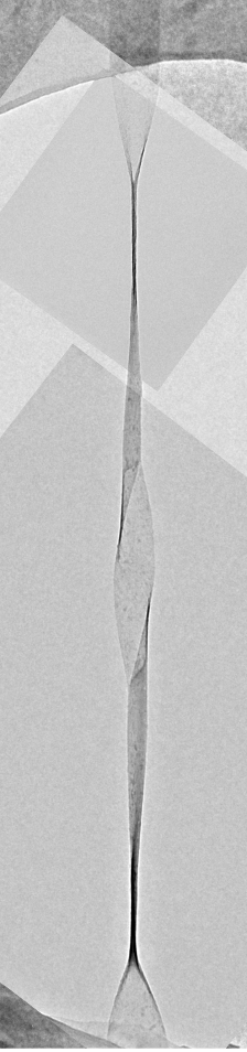 TEM of twisted PNR
Experimental Techniques
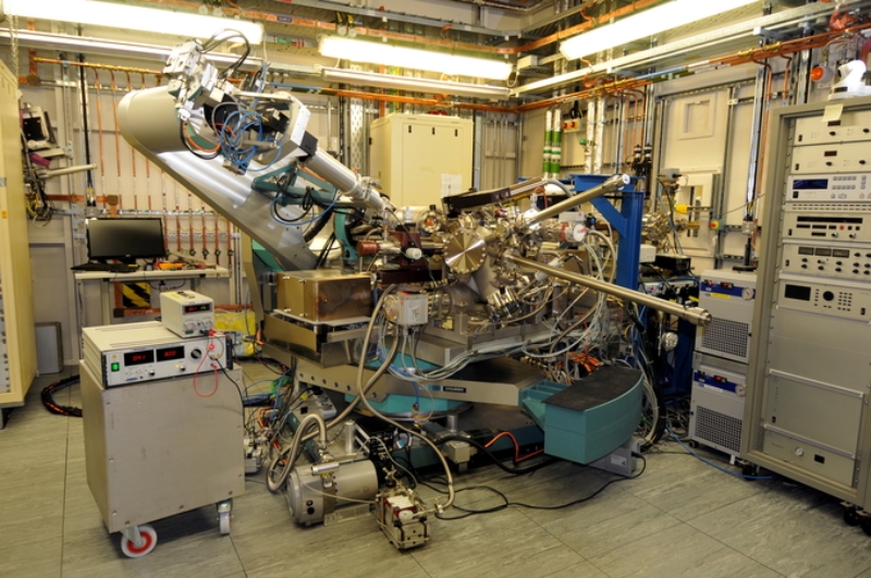 I05 ARPES beamline at Diamond Light Source, UK used for electronic structure measurements
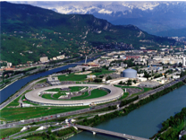 ESRF Synchnotron and ILL Neutron Source in Grenoble, France both used to probe the structure, excitations and dynamics
of the materials we create.
ESRF Synchnotron and ILL Neutron Source in Grenoble, France both used to probe the structure, excitations and dynamics
of the materials we create.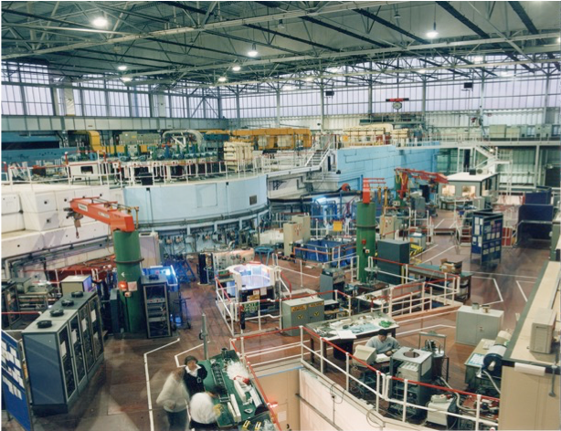 Target Station 1 at the ISIS Neutron and Muon Source, UK, we use elastic (wide and small angle), inelastic, quasi-elastic and muon spectroscopy.
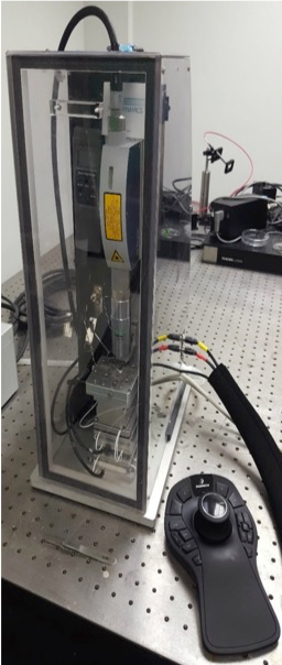 High speed AFM at Bristol built by Oliver Payton and Loren Picco
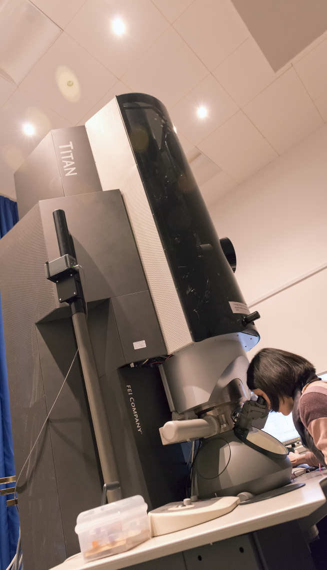 Titan electron microscope at Imperial College London
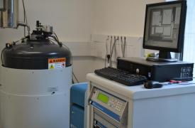 Physical Properties Measurement System, used to measure AC magnetistaion, resistivity and heat capacity as a function of field and temperature
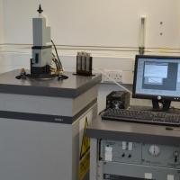 Magnetic Properties Measurement System, used to measure DC magnetistaion as a function of field and temperature
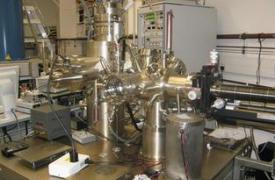 'Low temperature' UHV Scanning Tunnelling Microscope at the London Centre for Nanotechnology
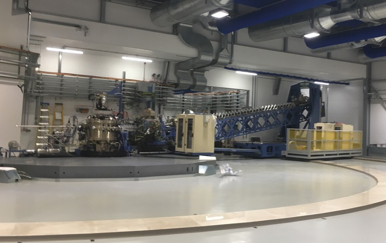 The incredible resonant inelastic X-ray scattering I21 beamline at Diamond light source.
 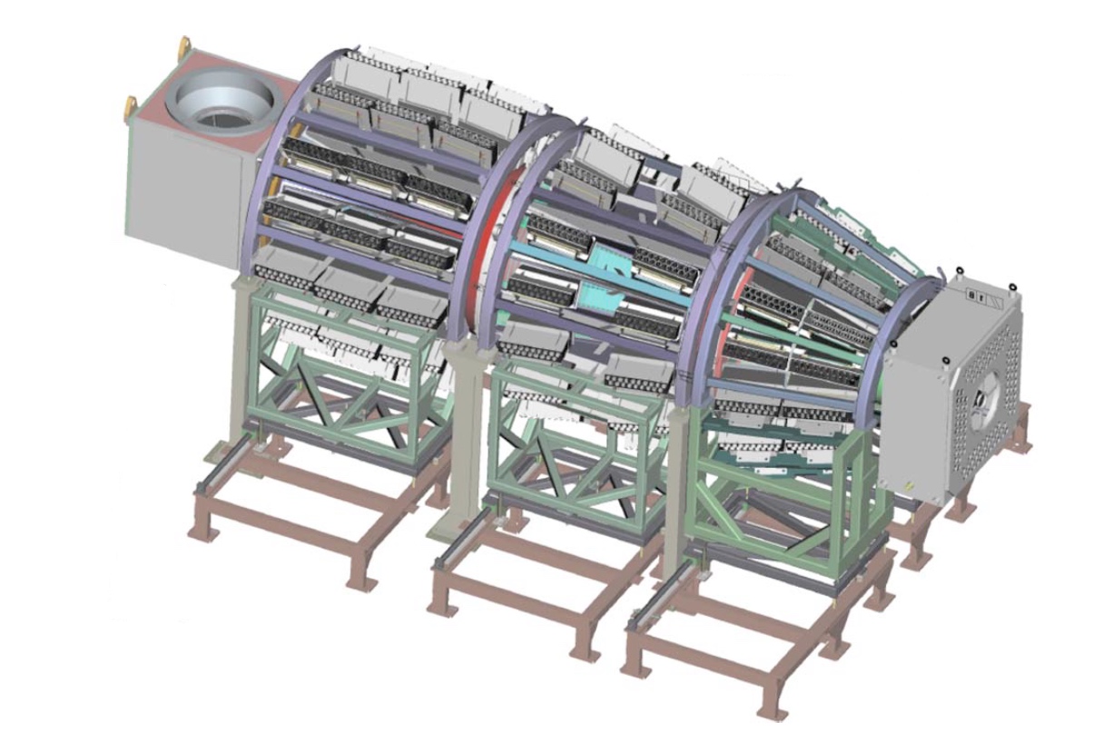 The NIMROD neutron diffractometer dectector bank at TS2 at ISIS Neutron and Muon Source, capable of measuring over an enormous Q-range for small and wide angle measurements.
We use this machine, in combination with modelling-based refinement of diffraction data to study local and long range order in liquids.
The NIMROD neutron diffractometer dectector bank at TS2 at ISIS Neutron and Muon Source, capable of measuring over an enormous Q-range for small and wide angle measurements.
We use this machine, in combination with modelling-based refinement of diffraction data to study local and long range order in liquids.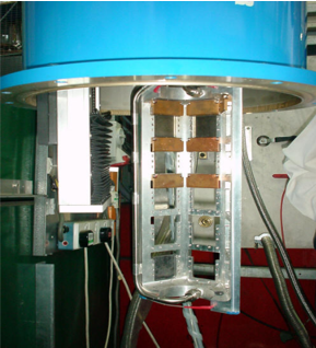 Candle stick and sample changer on the SANDALS instrument, ISIS Neutron and Muon Source
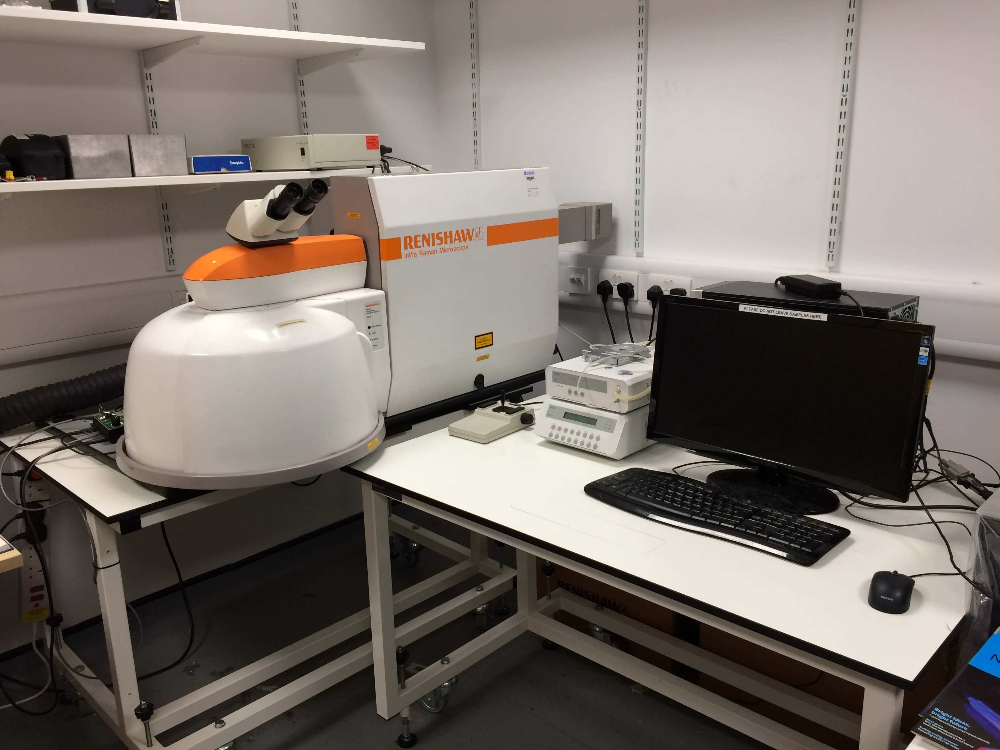 Our Raman spectrometer with mapping stage, three laser lines, low temperature capabilities
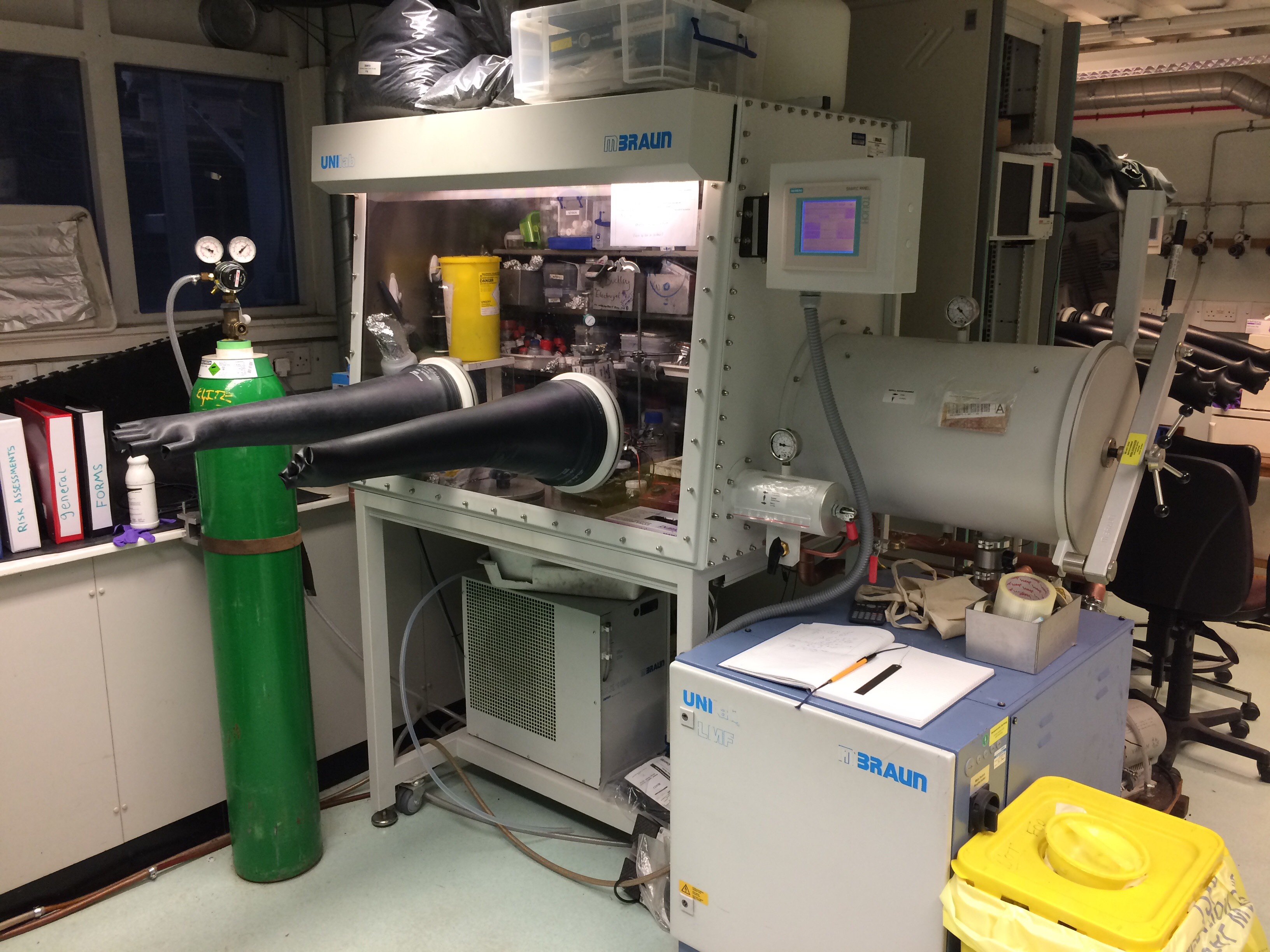 We have two gloveboxes for handling air-sensitive materials
Covers