| Research |
| Teaching |
| Publications |
| DensEl |
| ParaDens |
| Conquest |
| Links |
| Home |
When a Si(001) surface is covered in Bi and annealed at about 700K (just below the Bi desorption temperature), most of the Bi desorbs over time. However, the remaining Bi self-assembles into nanolines of quite startling straightness and perfection.
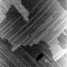
In the above image (which is 192nmx192nm), the Bi nanolines can be seen as straight, white lines. These lines typically extend for hundreds of nanometres, without a kink or a defect. This work was originally published in Surface Science 421, 397 (1999) and Physical Review B 59, 14868 (1999).
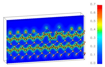
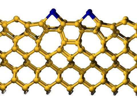
Despite their discovery, the structure of the Bi nanolines has remained a mystery, until recently. Using all the different experimental observations about the nanolines, and a combination of linear scaling tight binding (to perform rapid searches of many possible candidate structures) and density functional theory (to perform accurate calculations of energetics and electronic structure), we have identified the structure of the Bi nanolines (published as Physical Review Letter, 88, 226104 (2002)). This is shown below - first as a plain structure, then with a charge density plot
The electronic structure of the Bi nanolines has been explored in recent work (about to be submitted to Surface Science). We have confirmed that their bandgap is too large to permit conduction (and in fact they might well block conduction along the surface) and explained the origin of brightening in STM at low bias voltages. This work has been submitted to Surface Science, and is available as a preprint in gzipped postscript or PDF format.
The Haiku Structure for Bi nanolines
Charge Density for the Haiku Structure